PHILIPS DS1100 IPOD Docking speaker Disassembling and circuit diagram
PHILIPS DS1100
DISASSEMBLY DIAGRAM
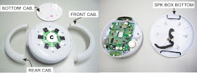
Dismantling of the Bottom Cabinet
Dismantling of the Bottom Cabinet
1) Remove 6 rubber feet A and 6 screws B as
indicated to loosen the Bottom Cabinet.
2) Remove 6 screws C as indicated to loosen the speaker box bottom
2) Remove 6 screws C as indicated to loosen the speaker box bottom
Dismantling of the PCB Board.
1)Remove 4 screws D as indicated to loosen the Main Board.
2)Remove 2 screws E as indicated to loosen the USB Socket Board.
1)Remove 4 screws D as indicated to loosen the Main Board.
2)Remove 2 screws E as indicated to loosen the USB Socket Board.
ICS USED IN THE CIRCUIT
PT6964 LED Driver IC
DESCRIPTION
PT6964 is an LED Controller driven on a 1/5 to 1/8 duty factor. 10 segment output lines, 4 grid output lines, 3 segment/ grid output lines, one display memory, control circuit, key scan circuit are all incorporated into a single chip to build a highly reliable peripheral device for a single chip microcomputer. Serial data is fed to PT6964 via a three-line serial interface. Housed in a 28 pins SOP Package, PT6964 pin assignments and application circuit are optimized for easy PCB Layout and cost saving advantages.
PT6964 is an LED Controller driven on a 1/5 to 1/8 duty factor. 10 segment output lines, 4 grid output lines, 3 segment/ grid output lines, one display memory, control circuit, key scan circuit are all incorporated into a single chip to build a highly reliable peripheral device for a single chip microcomputer. Serial data is fed to PT6964 via a three-line serial interface. Housed in a 28 pins SOP Package, PT6964 pin assignments and application circuit are optimized for easy PCB Layout and cost saving advantages.
FEATURES
# CMOS technology
# Low power consumption
3 Multiple display modes (10 segments, 7 grids to 13 segments, 4 grids)
# Key scanning (10 x 2 Matrix)
# 8-step dimming circuitry
# Serial interface for clock, data input, data output, strobe pins
# Available in 28 pins, SOP
# CMOS technology
# Low power consumption
3 Multiple display modes (10 segments, 7 grids to 13 segments, 4 grids)
# Key scanning (10 x 2 Matrix)
# 8-step dimming circuitry
# Serial interface for clock, data input, data output, strobe pins
# Available in 28 pins, SOP
PAM8403 FILTERLESS 3W CLASS-D
STEREO AUDIO AMPLIFIER IC
Description
The PAM8403 is a 3W, class-D audio amplifier. It offers low THD+N, allowing it to achieve high-quality sound reproduction. The new filterless architecture allows the device to drive the speaker directly, requiring no low-pass output filters, thus saving system cost and PCB area. With the same numbers of external components, the efficiency of the PAM8403 is much better than that of Class-AB cousins. It can extend the battery life, which makes it well-suited for portable applications. The PAM8403 is available in SOP-16 package
The PAM8403 is a 3W, class-D audio amplifier. It offers low THD+N, allowing it to achieve high-quality sound reproduction. The new filterless architecture allows the device to drive the speaker directly, requiring no low-pass output filters, thus saving system cost and PCB area. With the same numbers of external components, the efficiency of the PAM8403 is much better than that of Class-AB cousins. It can extend the battery life, which makes it well-suited for portable applications. The PAM8403 is available in SOP-16 package
Features
# 3W Output at 10% THD with a 4Ω Load and 5V Power Supply
# Filterless, Low Quiescent Current and Low EMI
# Low THD+N
# Superior Low Noise
# Efficiency up to 90%
# Short Circuit Protection
#Thermal Shutdown
# Few External Components to Save the Space and Cost
# Pb-Free Package
# 3W Output at 10% THD with a 4Ω Load and 5V Power Supply
# Filterless, Low Quiescent Current and Low EMI
# Low THD+N
# Superior Low Noise
# Efficiency up to 90%
# Short Circuit Protection
#Thermal Shutdown
# Few External Components to Save the Space and Cost
# Pb-Free Package
PIN CONFIGARATION
Pin Number
|
Pin Name
|
Function
|
1
|
+OUT_L
|
Left
Channel Positive Output
|
2
|
PGND
|
Power
GND
|
3
|
-OUT_L
|
Left
Channel Negative Output
|
4
|
PVDD
|
Power
VDD
|
5
|
MUTE
|
Mute
Control Input (active low)
|
6
|
VDD
|
Analog
VDD
|
7
|
INL
|
Left
Channel Input
|
8
|
VREF
|
Internal
analog reference, connect a bypass capacitor from VREF to GND.
|
9
|
NC
|
No
Connact
|
10
|
INR
|
Right
Channel Input
|
11
|
GND
|
Analog
GND
|
12
|
SHND
|
Shutdown
Control Input (active low)
|
13
|
PVDD
|
Power
VDD
|
14
|
-OUT_R
|
Right
Channel Negative Output
|
15
|
PGND
|
Power
GND
|
16
|
+OUT_R
|
Right
Channel Positive Output
|
SCHEMATIC DIAGRAM
CLICK ON THE IMAGES TO ZOOM IN


