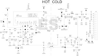
01-E421C8-PWE1XG TCL LCD TV POWER SUPPLY BOARD SCMATIC – LCD LED television power supply repair and service - FAN 7930P PFC DRIVER - FSL206MR POWER SWITCH - Manual service
Category: LCD Television Repair and Service
Contents of this article
- Power supply circuit diagram
- FAN7930 PFC Driver
- FS206MR Power Switch
TCL 01-E421C8-PWE1XG
FAN
7930P PFC DRIVER FSL206MR POWER SWITCH
Description
The FAN7930C is an active power factor correction (PFC)
controller for boost PFC applications that operate in critical conduction mode
(CRM). It uses a voltage- mode PWM that compares an internal ramp signal with the
error amplifier output to generate a MOSFET turn-off signal. Because the voltage-mode
CRM PFC controller does not need rectified AC line voltage information, it saves
the power loss of an input voltage-sensing network necessary for a current-mode
CRM PFC controller. FAN7930C provides over-voltage protection (OVP), open-feedback
protection, over-current protection (OCP), input-voltage-absent detection, and
under- voltage lockout protection (UVLO). The PFC-ready pin can be used to trigger
other power stages when PFC output voltage reaches the proper level with
hysteresis. The FAN793OC can be disabled if the INV pin voltage is lower than
0.45 V and the operating current decreases to a very low level. Using a new
variable on-time control method, total harmonic distortion (THD) is lower than
in conventional CRM boost PFC lCs.
PIN
CONFIGRATION
1 INV
This pin is the inverting input of the error amplifier.
The output voltage of the boost PFC converter should be resistively divided to
2.5 V.
2 RDY
This pin is used to detect PFC output voltage reaching a
pre-determined value. When output voltage reaches 89% of rated output voltage,
this pin is pulled HIGH, which is an (open-drain) output type.
3 COMP
This pin is the output of the transconductance error
amplifier. Components for the output voltage compensation should be connected
between this pin and GND.
4 CS
This pin is the input of the over-current protection
comparator. The MOSFET current is sensed using a sensing resistor and the
resulting voltage is applied to this pin. An internal RC filter is included to
filter switching noise.
5 ZCD
This pin is the input of the zero-current detection (ZCD)
block. If the voltage of this pin goes higher than 1.5 V, then goes lower than
1.4 V, the MOSFET is turned on.
6 GND
This pin is used for the ground potential of all the
pins. For proper operation, the signal ground and the power ground should be
separated.
7 OUT
This pin is the gate drive output. The peak sourcing and
sinking current levels are +500 mA and -800 mA, respectively. For proper
operation, the stray inductance in the gate driving path must be minimized.
8 Vcc
This is the IC supply pin. IC current and MOSFET drive
current are supplied using this pin.
FSL206MR
POWER SWITCH
Description
The FSL206MR integrated Pulse-Width Modulator (PWM) and
SenseFET is specifically designed for high- performance offline Switched-Mode
Power Supplies (SMPS) while minimizing external components. This device
integrates high-voltage power regulators that combine an avalanche-rugged
SenseFET with a Current-Mode PWM control block. The integrated PWM controller
includes: a 7.8V regulator, eliminating the need for auxilliary bias winding;
Under-Voltage Lockout (UVLO) protection; Leading-Edge Blanking (LEB); an
optimized gate turn- oniturn-off driver; EMI attenuator; Thermal Shutdown (TSD)
protection; temperature-compensated precision current sources for loop compensation;
soft-start during startup; and fault-protection circuitry such as Overload Protection
(OLP), Over-Voltage Protection (OVP), Abnormal Over-Current Protection (AOCP),
and Line Under-Voltage Protection (LUVP). The internal high-voltage startup switch
and the Burst- Mode operation with very low operating current reducethe power
loss in Standby Mode. As a result, it is possible to reach a power loss of
15OmW with no bias winding and 25mW (for FSL206MR) or 3OmW (for FSLZOBMRBN) with
a bias winding under no-load conditions when the input voltage is 265VAC.
PIN
CONFIGRATING
1 GND
Ground. SenseFET source terminal on primary side and
internal control ground.
2 Vcc
Positive Supply Voltage Input. Although connected to an
auxiliary transformer winding, current is supplied from pin 5 (VSTR) via an
internal switch during startup (see internal Block Diagram section). It is not
until \/CC reaches the UVLO upper threshold (BV) that the internal startup
switch opens and device power is supplied via the auxiliary transformer
winding.
3 VFB
Feedback Voltage. Non-inverting input to the PWM
comparator, with a 0.11mA current source connected internally and a capacitor
and opto-coupler typically connected externally. There is a delay while charging
external capacitor CFB from 2.4V to 5V using an internal 2.7uA current source.
This delay prevents false triggering under transient conditions, but allows the
protection mechanism to operate under true overload conditions.
4 LS
Line Sense Pin. This pin is used to protect the device
when the input voltage is lower than the rated input voltage range. If this pin
is not used, connect to ground.
5 Vsrn
Startup. Connected to the rectified AC line voltage
source. At startup, the internal switch supplies internal bias and charges an
external storage capacitor placed between the VCC pin and ground. Once \/CC
reaches 8V, all internal blocks are activated. After that, the internal high- voltage
regulator (HV REG) turns on and off irregularly to maintain \/CC at 7.8V.
6,7,8 Drain
Drain. Designed to connect directly to the primary lead
of the transformer and capable of switching a maximum of 650V. Minimizing the
length of the trace connecting these pins to the transformer decreases leakage
inductance.
POWER SUPPLY CIRCUIT
CLICK ON THE IMAGES TO ZOOM IN


