REPAIRING AND NOT THROWING AWAY

Richtige Fernseher haben Röhren!

Richtige Fernseher haben Röhren!

In Brief: On this site you will find pictures and technical information about Service Modes, Circuit Diagrams, Firmware Update procedure, Disassemble procedure, Universal remote control set-up codes, Troubleshooting and more....

If you go into the profession, you will obtain or have access to a variety of tech tips databases HERE IT IS Master Electronics Repair !.

These are an excellent investment where the saying: 'time-is-money' rules. However, to learn, you need to develop a general troubleshooting approach - a logical, methodical, method of narrowing down the problem. A tech tip database might suggest: 'Replace C536' for a particular symptom. This is good advice for a specific problem on one model. However, what you really want to understand is why C536 was the cause and how to pinpoint the culprit in general even if you don't have a service manual or schematic and your tech tip database doesn't have an entry for your sick TV or VCR.

While schematics are nice, you won't always have them or be able to justify the purchase for a one-of repair. Therefore, in many cases, some reverse engineering will be necessary. The time will be well spent since even if you don't see another instance of the same model in your entire lifetime, you will have learned something in the process that can be applied to other equipment problems.
As always, when you get stuck, checking out a tech-tips database may quickly identify your problem and solution.In that case, you can greatly simplify your troubleshooting or at least confirm a diagnosis before ordering parts.

Happy repairing!
Today, the West is headed for the abyss. For the ultimate fate of our disposable society is for that society itself to be disposed of. And this will happen sooner, rather than later.

How to use the site:

- If you landed here via any Search Engine, you will get what you searched for and you can search more using the search this blog feature provided by Google. You can visit more posts scrolling the left blog archive of all posts of the month/year,
or you can click on the main photo-page to start from the main page. Doing so it starts from the most recent post to the older post simple clicking on the Older Post button on the bottom of each page after reading , post after post.

You can even visit all posts, time to time, when reaching the bottom end of each page and click on the Older Post button.

- If you arrived here at the main page via bookmark you can visit all the site scrolling the left blog archive of all posts of the month/year pointing were you want , or more simple You can even visit all blog posts, from newer to older, clicking at the end of each bottom page on the Older Post button.
So you can see all the blog/site content surfing all pages in it.

- The search this blog feature provided by Google is a real search engine. If you're pointing particular things it will search IT for you; or you can place a brand name in the search query at your choice and visit all results page by page. It's useful since the content of the site is very large.

Note that if you don't find what you searched for, try it after a period of time; the site is a never ending job !

..............The bitterness of poor quality is remembered long after the sweetness of todays funny gadgets low price has faded from memory........ . . . . . .....
Don't forget the past, the end of the world is upon us! Pretty soon it will all turn to dust!

©2010, 2011, 2012, 2013, 2014 Frank Sharp - You do not have permission to copy photos and words from this blog, and any content may be never used it for auctions or commercial purposes, however feel free to post anything you see here with a courtesy link back, btw a link to the original post here , is mandatory.
All posts are presented here for informative, historical and educative purposes as applicable within fair use. NOTHING HERE IS FOR SALE !

Showing posts with label POWER-SUPPLY. Show all posts

Thursday, 15 October 2020

HOW TO CALCULATE SMPS FLYBACK TRANSFORMER DESIGN

 A switched-mode power supply (switching-mode power supply, switch-mode power supply, switched power supply, SMPS, or switcher) is an electronic power supply that incorporates a switching regulator to convert electrical power efficiently


SMPS stands for switch-mode power supply unit. The properties of an SMPS transformer are highly dependent on the frequency in which they operate. High switching frequency opens up the possibilities to choose smaller SMPS transformers these high frequency, SMPS transformers uses ferrite cores.

The transformer core design is the most important thing in an SMPS transformer construction. A core has a different type of AL (Ungapped core inductance Coefficient) depending on the core material, core size, and core type. Popular type of core material are N67, N87, N27, N26, PC47, PC95, etc. Also, the manufacturer of ferrite cores provides detailed parameters in the datasheet, which will be useful while selecting the core for your transformer


Bobbin

A bobbin is the housing of cores and windings. A bobbin has an effective width which is essential to calculate the wire diameters and the construction of the transformer. Not only this, a bobbin of a transformer also has a dotted mark which provides the information of primary windings.
 

Primary winding

The SMPS transformer winding will have a primary winding and a minimum of one secondary winding, based on the design it might hav more secondary winding or an auxiliary winding. The primary winding is the first and innermost winding of a transformer. It is directly connected to the primary side of an SMPS. Usually number of winding on primary side is more than other windings of the transformer. Finding the Primary winding in a transformer is easy; one just needs to check the dot side of the transformer for the primary winding. It is generally situated across the high voltage side of the mosfet.

In an SMPS schematic, you can notice the high voltage DC from the high voltage capacitor connected with the primary side of the transformer and the other end is connected with the power driver (Internal mosfet drain pin) or with a separate high voltage MOSFET's drain pin.


Secondary winding

Secondary winding converts the voltage as well as the current on the primary side to the required value. Finding out the secondary output is a bit complex as in some SMPS designs the transformer usually has multiple secondary outputs. However, the output or low voltage side of an SMPS circuit is generally connected to the secondary winding. One side of the secondary winding is the DC, GND and the other side is connected across the output diode.

As discussed, an SMPS transformer can have multiple outputs. Therefore an SMPS transformer can also have multiple secondary windings.


 Some people may still be confused about how the rules for the SMPS transformer or commonly called ferrite transformers.

Previously there were several rules for selecting wire diameters based on the frequencies used.
AWG Cable transformer SMPS
After knowing the wire that is used based on the frequency of the MOSFET driver that is used now we see first the formula determines the primary winding (Np).
How to Calculate SMPS Transformer - Formula
Description
Npri = primary winding
Vin = Effective Input Voltage
f = frequency
Bmax = maximum flux density 1200 - 2000
Ac = Effective Cross Sectional Area (see datasheet of each type of transformer core (example EI33 = 1.19, ETD39 = 1.25).

For example, the above formula is specifically for push-pull topology.

For example, I want to make an inverter transformer with specifications:
Effective Vinput = 12v
Minimum Vinput = 10,5v
Max output = 330v
Normal Vout = 220v

Driver frequency = 50KHz or 50000Hz
then the primary (Np) and secondary (Ns) are?
I previously set the Bmax I want to use is 1600 (range Bmax 1200-2000) and uses EI33 core type with Ac 1.19

Np = (12v x100000000) / (4x50000x1600x1,19)
Np = 3.15 my turn rounds to 3 turns

check the Bmax value again not to be less than or more than the adjusted range above. then if I turn rounds into 3 (Np = 3).
How to Calculate SMPS Transformer - Formula Bmax

Bmax = (12v x100000000) / (4x50000x3x1,19)
Bmax = 1680 (still in the range 1200-2000)

Now we calculate Primary Turn (Ns). because the output voltage can be adjusted or stabilized by setting the percentage duty cycle, if there is a voltage input drop to a minimum of 10.5v, the duty will increase to a maximum of 98% to maintain normal output stability at 220v or at least above 200v. For that N = 330v / (10,5v x 98% duty) = 32 so
Ns = N x Np
Ns = 32 x 3
Ns = 96 turns
How to winding SMPS Transformator

To optimize the voltage-current, you can double the number of wires in accordance with the power and capacity of the bobbin.
Suppose you make a transformer with an output power of 300 watts, then 300watt / 220v = 1.4Amper and see the wire that can be used with a 50KHz frequency in the AWG table above. for example the wire used is 0.5mm then 1.4 Amp / 0.5 = 2.8 or rounded down or upward to be 2 or 3 double wire and of course the coil must be 2 or 3 times more primary wire used than secondary because Vin 12v then 300w / 12v = 25A so that the primary transformer wire does not overheat it must be joined into several wires in accordance with the bobbin ability or the capacity of the transformer bobbin.

12V 50W SWITCHING REGULATOR CIRCUIT SCHEMATIC DIAGRAM

 By definition, a switch mode power supply (SMPS) is a type of power supply that uses semiconductor switching techniques, rather than standard linear methods to provide the required output voltage. The basic switching converter consists of a power switching stage and a control circuit.

 
The schematic diagram below shows a simple trivial low-cost 12 volt DC 50W off-line SMPS switching power supply circuit. It can be used for DIY home projects or to learn operation of flyback converters. This PSU can work over a universal input AC line range 90-264 VAC. It provides a nominal 12V DC output at more than 4A load. Line and load regulation is better then 0.5%.
The unit has over current, over temperature and over voltage protections, as well as passive inrush current limiting. Output ripple are approximately 0.2 V peak to peak in the range 0 to 20 MHz. If you need to get lower ripple, you may put an additional output capacitor or an LC filter outside of the feedback loop. This project is a modification of a 24V circuit that I've designed many years ago as a consultant for a small company. That company wanted a plug-in replacement to a cheap off-the-shelf AC to DC power supply, which had a long lead time. By the time I've completed the design and built a proto, they found the off-the-shelf part elsewhere in stock. So, they never proceeded with a manufacturing of this module. Accordingly, I have not tested this design beyond a basic DVT. You can build this circuit for personal use (at your own risk of course). But you are not allowed to republish the content of this page anywhere or use it for commercial purposes without my permission.

SAFETY WARNING.

 
To safely test or troubleshoot this circuit it is recommended to power it via an isolation transformer or from an isolated AC source. Also note that an offline single-transistor flyback converter generates internal voltages which may reach 600 V. Don't try to play with this circuit unless you are of a legal age, understand power electronics and know how to deal safely with high voltage. You may want to take our quick power supply safety quiz.


12V 50W Switching Regulator Circuit Diagram


CIRCUIT OPERATION.

This AC to DC power supply utilizes a fly back, which is the simplest SMPS converter topology. It uses an 800V/11A MOSFET (Q1) as the switching device and PWM controller UC3844AN (U3). The input section includes a fuse, EMI filter, inrush current limiting NTC resistor R1, a full bridge rectifier CR1, and a DC bus filter capacitor C2.

The initial start-up current for the PWM IC is provided by "bleeding" resistors R7, R8 that allow small current which charges the Vcc capacitor C7.

When the Vcc pin of U3 reaches the positive under voltage lockout threshold (typically 14V-16V), the IC starts to operate and will be driving ON and OFF the switch Q1 via a gate drive resistor R4 at a fixed frequency (in this circuit it is 100 kHz). When Q1 turns on, the DC bus voltage is applied across the transformer T1 primary winding, current through the transformer primary ramps up and energy is accumulated in the transformer's magnetic field. Diodes D4 and D7 during this time interval are reversed biased. When Q1 turns off, the energy stored in the magnetic field causes the voltages across all winding to reverse polarity. As a result, output rectifiers D4 and D7 conduct and the stored energy is transferred to the output and to the bias circuit.Once the converter is started, the bias for the control PWM comes from the bias winding of the transformer.

The secondary side feedback control loop uses a TL431 precision shunt regulator D1 as both the reference and an error amplifier. It compares divided output voltage to D1's internal reference 2.5V. An optocoupler U1 feeds the current proportional to the error signal across the transformer galvanic isolation boundary back to the primary PWM. If accurate regulation of the output is not required, the feedback can be taken from the bias voltage at C9 and fed via a divider into feedback pin 2.

Primary current in T1 is sensed by a resistor R6. This current sense voltage is applied through a spike filter to the current sense terminal of U3, where it is compared against the scaled down error signal at compensation pin 1. When current sense voltage ramp reaches 1/3×(Vpin1-1), the pulse is terminated and Q1 turns off.
Zener diode D6 with optocoupler U2 provide a non-latching output's overvoltage protection.

Thermal switch shuts down the power supply when temperature on the MOSFET heatsink exceeds 95-100 oC.

Here is complete BOM. Note that it was compiled more than ten years ago. Some part numbers may need replacements.

Printed Circuit Boards:

12V 50W Switching Regulator Circuit Diagram


The transformer design may look unusual. Note that a flyback transformer operates as an inductor: it accumulates energy in the magnetic field during ON period of Q1. Then it transfers it (minus losses) into the secondaries during the OFF period of Q1. In order to store energy efficiently with minimal physical size, a non-magnetic gap is needed in series with a high permeability magnetic core material. Flyback transformer design usually uses ferrite cores with a physical gap, or powdered metal cores with an inherently present distributed gap. Gapped ferrites normally feature lower losses, but they have abrupt saturation curve. Powder cores have higher losses, but their B(H) curve is soft. Among other form factors, toroidal transformers have lowest leakage inductance. In this PSU the transformer is made with KoolM powder toroidal core. Proper winding phasing is critical in flybacks just like in all single-ended converters. If windings are misphased the circuit will not work or may simply blow up. Refer to the schematic and winding diagram above for proper transformer installation. All coils in this design have to be made of wire with two or more layers of Teflon insulation to assure reinforced insulation between primary and secondary.

LGP42-09LF, LGP42-09LH LCD TV - EAY57681301(FHD), EAY57681302(HD) POWER BOARD SCHEMATIC DIAGRAM USING STR W6252, ICE2PCS06G, 2SK3797


General Description


The STR-W6200D series are power ICs for switching power supplies, incorporating a power MOSFET and a current mode PWM controller IC in one package. Includ- ing a startup circuit and a standby function in the controller, the product achieves low power consumption, low standby power, and high cost-effectiveness in power supply systems, while reducing external components.
Features and Benefits
▪ TO-220 fully-molded package with 6 pins
▪ Current mode PWM control
▪ PWM and frequency modulation functions: reduces EMI
noise, simplifies EMI filters, and cuts cost by external part
reduction
▪ Built-in Slope Compensation circuit: avoids subharmonic
oscillation
▪ Automatic Standby Mode function (Input Power < 40
mW at no load)
▫ Normal operation: PWM mode
▫ Light load operation: Standby mode (burst oscillation)
▪ Built-in Audible Noise Suppression function during
Standby mode
▪ Built-in startup circuit: reduces power consumption in
standby operation, and eliminates external components
▪ Bias-Assist function: improves startup operation,
suppresses VCC pin voltage drop in operation, and allows
use of smaller VCC capacitor
▪ Built-in Leading Edge Blanking function
▪ Protection Functions:
▫ Overcurrent Protection function (OCP); pulse-by-pulse,
built-in compensation circuit to minimize OCP point
variation on AC input voltage
▫ Overload Protection function (OLP); auto restart, built-in
timer, reduces heat during overload condition, and few
external components required
▫ External Latch Protection function (ELP): latched
shutdown by external signal
▫ Overvoltage Protection function (OVP): latched
shutdown
▫ Thermal Shutdown function (TSD); latched shutdown


Electrical characteristics

Intermittent Operation stability test:  The switching regulator shall ON-OFF for 20,000 time at an interval of 10 sec at maximum load, after that electrical characteristics shall be satisfied.

Low temperature operation:  The switching regulator is left at the operating guarantee minimum temperature for 2 hours without applying electricity.  After that power shall be turned on, and then the electrical characteristics shall be satisfied.

Low temperature Storage test Leave at low temperature:  The switching regulator is left at minimum storage temperature for 96 hours or more.  Then the switching regulator is left at a room temperature and humidity for 1hour or more, after that electrical characteristics shall be satisfied.

Schematic


Connector voltages

Bottom and top view


Wednesday, 14 October 2020

UNIVERSAL DC POWER SUPPLY SCHEMATIC DIAGRAM

 Shown below is a supply that will use any of the LM78XX series of voltage regulators. The transformer in the circuit will vary depending on which regulator you use. For voltages from 5 to 12 use a transformer with output of 18vac. With voltages from 15 to 24 use a transformer of 30vac. The first capacitor in the circuit may need to vary if you are supplying more current to the load. Typically it will be 2000uf for every amp of current.

www.streampowers.blogspot.com

BUILDING A LED HALOGEN LAMP FOR MOTORBIKE HEAD-LAMP REPLACEMENT

The post explains a simple 21 watt LED lamp circuit module which can be used as a direct replacement for a standard halogen lamp in motorcycles.


The proposed "halogen" LED lamp replacement module image can be seen below:


Conventional filament type halogen lamp is shown below:

The image at the top shows an example LED lamp replacement for a standard halogen bulb fitting shown below it.
With the easy and extensive availability of LEds, today it's quite possible to make any desired LED lamp module at home for replacing other forms of less efficient lamp options.
So here we'll discuss how to make the proposed halogen LED lamp replacement circuit. Let's learn the procedures:
Referring to the above image, we can see the LEDs are wired over 7 separate PCBs and then wired together to form one single module.
Each board can be seen with 3 LEDs each, constituting a total of 21 LEDs.
3nos LEDs are selected because the supply 12V available from the vehicle allows only 3nos to be connected in series, and series connection facilitates sharing the same current across the three LEDs.
Now since more than 3nos. of LEds cannot be accommodated in series, 7 such strings are connected in parallel with each other for achieving the desired 21 watts.

The above assembly must be done over a well designed heatsink cored glass epoxy PCB.
The entire configuration may be tightly fixed over an thick hexagonal aluminum cylindrical former or base to form the proposed halogen LED module unit. The aluminum will hep to sink the generated heat from the LEDs.

The above unit will strictly require a current controlled driver circuit which can be understood with the following points:

We once again take the help of the versatile LM338 IC for the required current control function.

Referring to the circuit diagram we ca see it in it's simplest current limiting mode. The LEDs consume around 2.5 amps together which is never allowed to exceed by the IC keeping the unit safe from the issue.
Aluminum mount or base design for fixing the LED PCB assembly


Comparison Between Conventional Halogen lamp and LED Halogen lamp Output


Output                              Conventional Incandescent    LED Halogen Lamp
Specs                               Halogen
     
Nominal wattage              55 watts                                       21 watts

Nominal voltage               12V                                               12V

Test voltage                     13.2V                                            13.2V


Color temperature          3200K                                           6000K

Luminous flux                 1500lm                                         2500lm

Tuesday, 13 October 2020

PHILIPS 50PUG6513, PHILIPS 55PUG6513, PHILIPS 65PUG6713 HOW TO ENTER THE SERVICE MODE, SOFTWARE UPDATE PROCEDURE , POWER SUPPLY SCHEMATICS AND MORE

Applicable to Philips 50PUG6513/78, 50PUG6513/77, 55PUG6513/78, 65PUG6703/77, 55PUG6703/77 Chassis TPM18.6L LA, Platform MTK5802

Mains power : AC 220-240V +/-10%

Power saving features: Eco mode, Picture mute (for radio), Auto switch-off timer, Eco settings menu.

Diagonal screen size

55PUG6703: 139 cm / 55 inch

65PUG6703: 164 cm / 55 inch

55PUx6513: 139 cm / 55 inch

 50PUx6513: 126 cm / 50 inch

 PAL,NTSC,SECAM

 480i – 24Hz, 25Hz, 30Hz, 50Hz, 60Hz

 480p– 24Hz, 25Hz, 30Hz, 50Hz, 60Hz

 576i – 24Hz, 25Hz, 30Hz, 50Hz, 60Hz

 576p– 24Hz, 25Hz, 30Hz, 50Hz, 60Hz

 720p– 24Hz, 25Hz, 30Hz, 50Hz, 60Hz

 1080i– 24Hz, 25Hz, 30Hz, 50Hz, 60Hz

 1080p – 24Hz, 25Hz, 30Hz, 50Hz, 60Hz

Supported Input Resolution – Computer

 640 x 480 – 60Hz

 800 x 600 – 60Hz

 1024 x 768 – 60Hz

 1280 x 800 – 60Hz

 1280 x 960 – 60Hz

 1280 x 1024 – 60Hz

 1366 x 768 – 60Hz

 1440 x 900 – 60Hz

 1920 x 1080 – 60Hz

 3840 x 2160 – 60Hz

HDMI – UHD

(HOME) > Settings > General settings > HDMI Ultra HD

This TV can display Ultra HD signals. Some devices connected with HDMI – do not recognize a TV with Ultra HD and might not work correctly or show distorted picture or sound.

To avoid the malfunctioning of such a device, you can set the signal quality to a level the device can handle. If the device is not using Ultra HD signals, you can switch off Ultra HD for this HDMI connection.
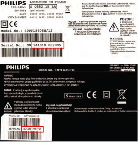
Identification: The bottom line of a type plate gives a 14-digit serial number. Digits 1 and 2 refer to the production centre (e.g. SN is Lysomice, RJ is Kobierzyce), digit 3 refers to the B.O.M. code, digit 4 refers to the Service version change code, digits 5 and 6 refer to the  production year, and digits 7 and 8 refer to production week (in example below it is 2010 week 10 / 2010 week 17). The 6 last digits contain the serial number.


It should be noted that on the European Service website, “Alternative BOM” is referred to as “Design variant”.

The third digit in the serial number (example:

AG2B0335000001) indicates the number of the alternative B.O.M. (Bill Of Materials) that has been used for producing the specific TV set. In general, it is possible that the same TV model on the market is produced with e.g. two different types of displays, coming from two different suppliers. This will then result in sets which have the same CTN (Commercial Type Number; e.g. 28PW9515/12) but which have a different B.O.M. number.

By looking at the third digit of the serial number, one can identify which B.O.M. is used for the TV set he is working with. If the third digit of the serial number contains the number “1” (example: AG1B033500001), then the TV set has been manufactured according to B.O.M. number 1. If the third digit is a “2” (example: AG2B0335000001), then the set has been produced according to B.O.M. no. 2. This is important for ordering the correct spare parts.

Service Modes

The Service Mode feature is split into following parts:

 Service Alignment Mode (SAM).

 Factory Mode.

 Customer Service Mode (CSM).SAM and the Factory mode offer features, which can be used by the Service engineer to repair/align a TV set.

SAM and the Factory mode offer features, which can be used by the Service engineer to repair/align a TV set. Some features are:

Make alignments (e.g. White Tone), reset the error buffer(SAM and Factory Mode).

 Display information (“SAM” indication in upper right corner of screen, error buffer, software version, operating hours, options and option codes, sub menus).

The CSM is a Service Mode that can be enabled by the consumer. The CSM displays diagnosis information, which the customer can forward to the dealer or call centre. In CSM mode, “CSM”, is displayed in the top right corner of the screen. The information provided in CSM and the purpose of CSM is to:

 Increase the home repair hit rate.

 Decrease the number of nuisance calls.

 Solved customers’ problem without home visit.

Note: For the new model range, a new remote control (RC) is used with some renamed buttons. This has an impact on the activation of the Service modes.

For instance the old “MENU” button is now called “HOME” (or is indicated by a “house” icon).

Service Alignment Mode (SAM)

How to Activate SAM

To activate SAM, use one of the following methods:

 Press the following key sequence on the remote control transmitter: “062596”, directly followed by the “INFO/OK” button. Do not allow the display to time out between entries while keying the sequence.

Or via ComPair.

After entering SAM, the following items are displayed, with “SAM” in the upper right corner of the screen to indicate that the television is in Service Alignment Mode.

How to Navigate

 In the SAM menu, select menu items with the UP/DOWN keys on the remote control transmitter. The selected item will be indicated. When not all menu items fit on the screen, use the UP/DOWN keys to display the next/previous menu items.

 With the “LEFT/RIGHT” keys, it is possible to:

– (De) activate the selected menu item.

– (De) activate the selected sub menu.

– Change the value of the selected menu item.

When you press the MENU button once while in top level SAM, the set will switch to the normal user menu (with the SAM mode still active in the background).

How to Store SAM Settings

To store the settings changed in SAM mode (except the RGB Align settings), leave the top level SAM menu by using the POWER button on the remote control transmitter or the television set. The mentioned exceptions must be stored separately via the STORE button.

How to Exit SAM

Use one of the following methods:

 Switch the set to STANDBY by pressing the mains button on the remote control transmitter or the television set.

 Via a standard RC-transmitter, key in “00” sequence.

Note: When the TV is switched “off” by a power interrupt while in SAM, the TV will show up in “normal operation mode” as soon as the power is supplied again. The error buffer will not be cleared.

Remark:

1. Press following Key Combination to reset the “Op Hour”: “Menu/Home” + “101011” on the remote control transmitter.

2. Under main menu “NVM editor”, select “Service Data”, you can use the UP/DOWN keys to view and change the set Type number, the set Production Number or the 18AC of a part.(The NVM-editor still has the same function as before, alpha-numeric entry.)

Factory mode:

 Displaying and or changing Panel ID information.

 Displaying and or changing Tuner ID information.

 Error buffer clearing.

 Various software alignment settings.

 Testpattern displaying.

 Public Broadcasting Service password Reset.

 etc.

To activate the Factory mode, use the following method:

 Press the following key sequence on the remote control transmitter: from the “menu/home” press “1999”, directly followed by the “Back/Return” button. Do not allow the display to time out between entries while keying the sequence.

After entering the Factory mode, we can see many items displayed, use the UP/DOWN keys to display the next/previous menu items.

How to Exit the Factory mode

 Select EXIT_FACTORY from the menu and press the “OK” button.

Note: When the TV is switched “off” by a power interrupt, or normal switch to “stand-by” while in the factory mode, the TV will show up in “normal operation mode” as soon as the power is supplied again. The error buffer will not be cleared.

Customer Service Mode (CSM)

The Customer Service Mode shows error codes and information on the TVs operation settings. The call centre can instruct the customer (by telephone) to enter CSM in order to identify the status of the set. This helps the call centre to diagnose problems and failures in the TV set before making a service call.

The CSM is a read-only mode; therefore, modifications are not possible in this mode.

How to Activate CSM

To activate CSM, press the following key sequence on a standard remote control transmitter: “123654” (do not allow the display to time out between entries while keying the sequence). After entering the Customer Service Mode, the following items are displayed. use the Right/Left keys to display the next/previous menu items.

Note: Activation of the CSM is only possible if there is no (user) menu on the screen.

How to Navigate

By means of the “CURSOR-DOWN/UP” knob (or the scroll wheel) on the RC-transmitter, can be navigated through the menus.

How to Exit CSM

To exit CSM, use one of the following methods.

 Press the MENU/HOME button on the remote control transmitter.

 Press the POWER button on the remote control transmitter.

 Press the POWER button on the television set.

Software Upgrading, Error code and Panel Code.

The following update is for .pkg file.

1. Rename the file to “upgrade_loader.pkg”.

2. Prepare a USB memory (File format: FLAT, Size: 1G~8G).

3. Copy the software to USB flash disk (root directory).

4. Switch off the TV and Insert the USB memory stick that contains the software update files in one of the TV’s USB 2.0 port.

Note: It contains USB3.0 port, if connect on it, the software may can’t be detected.

5. Switch on the TV. The TV will detect the USB memory s tick automatically. Then a window jumps out as below:

6. When the TV software is updated, the TV will turn on again automatically. Remove your USB flash drive.

7. We can enter in CSM or Factory mode to check the current software version.

The following update is for .upg file.

Step 1: Ready for F/W Upgrade

1. Rename the file to “autorun.upg”.

2. Prepare a USB memory (File format: FLAT, Size: 1G~8G).

3. Copy the software to USB flash disk (root directory).

4. Switch on the TV and Insert the USB memory stick that contains the software update files in one of the TV’s USB 2.0 port.

Note the version of this F/W before you change the software file name.

Step 2: F/W Upgrade

Press [Quick settings], then Choose [Update Software] in the Settings menu

2. Choose [Local Updates], then press OK.

3. Select the file that you downloaded and press OK.

4. Choose [Update], then choose [Start] on following step.

5. Upgrade in progress.

Step 3: Check the SW version.

After burning software, TV will restart

2. Press “123654”, enter Customer Service Mode to check if the software version is correct.

Caution: Please make sure that software upgrade is finished before unplug the USB and AC power.


Error Code

Error codes are required to indicate failures in the TV set. In principle a unique error code is available for every:

• Activated (SW) protection.

• Failing I2C device.

• General I2C error.

The last five errors, stored in the NVM, are shown in the Service menu’s. This is called the error buffer.

The error code buffer contains all errors detected since the last time the buffer was erased. The buffer is written from left to right. When an error occurs that is not yet in the error code buffer, it is displayed at the left side and all other errors shift one position to the right.

An error will be added to the buffer if this error differs from any error in the buffer. The last found error is displayed on the left.

An error with a designated error code never leads to a deadlock situation. It must always be diagnosable (e.g. error buffer via OSD or blinking LED).

In case a failure identified by an error code automatically results in other error codes (cause and effect), only the error code of the MAIN failure is displayed.

How to Read the Error Buffer.

You can read the error buffer in following ways:

On screen via the SAM/CSM (if you have a picture).

Example:

– ERROR: 000 000 000 000 000: No errors detected

– ERROR: 013 000 000 000 000: Error code 13 is the last and only detected error

– ERROR: 034 013 000 000 000: Error code 13 was detected first and error code 34 is the last detected (newest) error

 Via the blinking LED procedure (when you have no picture).

Error codes overview

In this chassis only “layer 2” error codes are available and point to problems on the SSB. They are triggered by LED blinking when CSM is activated. Only the following layer 2 errors are defined:

How to Clear the Error Buffer.

The error code buffer is cleared in the following cases:

By using the CLEAR command in the SAM menu

By using the CLEAR command in the Factory mode:

By using the following key sequence on the remote control transmitter: “062599” directly followed by the OK button.

If the contents of the error buffer have not changed for 50 hours, the error buffer resets automatically.

Note: If you exit SAM by disconnecting the mains from the television set, the error buffer is not reset.

Set Option Code

Press the following key sequence on a standard RC transmitter: “062598” directly followed by MENU and “xxx”, where “xxx” is a 3 digit decimal value of the panel type: see column “Set Option Code” in below tab. After resetting the Display Code, restart the set immediately.

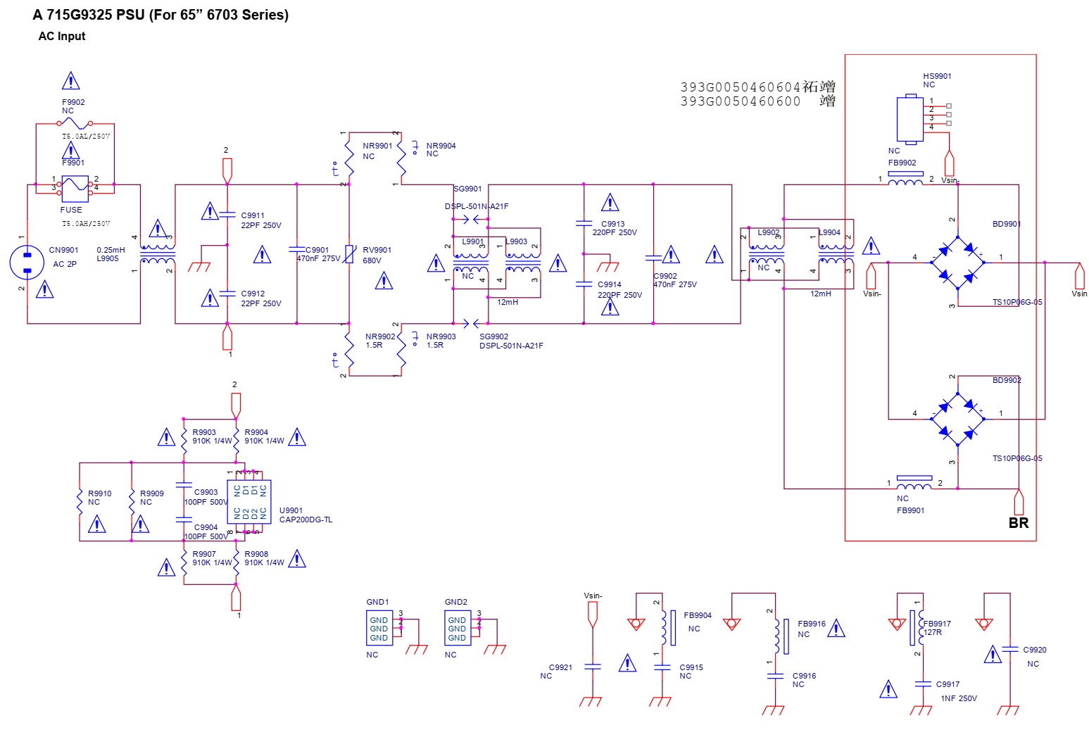
Power board schematic


A 715G9309 PSU(For 55” 6703 Series)


A 715G8967 PSU (For 6513 Series)


A 715G9325 PSU (For 65” 6703 Series)


B 715G8709SSB POWER - 2K17 MT5802 platform


LG 50PJ350 PLASMA TV POWER SUPPLY BOARD TROUBLESHOOTING / DIAGNOSE , VOLTAGES DETAIL

 Adjustment Notice:  All adjustments (DC or Waveform) are adjusted in WHITE WASH.  Customer’s Menu, Select “Options”, select “ISM” select “WHITE WASH”

It is critical that the DC Voltage adjustments be checked when;
1) SMPS, Y-SUS or Z-SUS board is replaced.
2) Panel is replaced, Check Va/Vs since the SMPS does not come with new panel.
3) A Picture issue is encountered.
4) As a general rule of thumb whenever the back is removed.

ADJUSTMENT ORDER “IMPORTANT” DC VOLTAGE ADJUSTMENTS
1) POWER SUPPLY: VS, VA (Always do first)
2) Y-SUS: Adjust –Vy, VSC
3) Z-SUS: Adjust Z-Bias (VZB)
WAVEFORM ADJUSTMENTS
1) Y-SUS: Set-Up, Set-Down

The Waveform adjustment is only necessary
1) When the Y-SUS board is replaced
2) When a “Mal-Discharge” problem is encountered
3) When an abnormal picture issues is encountered.


SWITCH MODE POWER SUPPLY [SMPS] SECTION

This Section of the Presentation will cover troubleshooting the Switch Mode Power Supply for the Single Scan Plasma. Upon completion of the section the technician will have a better understanding of the operation of the Power Supply Circuit and will be able to locate voltage and test points needed for troubleshooting and alignments.
DC Voltages developed on the SMPS
Adjustments VA and VS

Always refer to the Voltage Sticker located on the back of the panel, in the upper Left Hand side for the correct voltage levels for the VA, VS, -VY, VSC, and Z Bias as these voltages will vary from Panel to Panel even in the same size category.
Set-Up and Ve are just for Label location identification and are not adjusted in this panel.

SMPS Part Number: EAY60968701
Check the silk screen label on the top center of the Power Supply board to identify the correct part number. (It may vary in your specific model number).

Operation of this Power Supply.

The Switch Mode Power Supply Board Outputs to the :

Y-SUS Board

VS: Drives the Display Panel’s Horizontal Electrodes.

VA: Drives the Display Panel’s Horizontal Electrodes.

M5V: Used to develop Bias Voltages on the Y-SUS then routed to the Control board and then to the Z-SUS Board.

Z-SUS Board

VS: VS is routed to the Y-SUS first then to the Z-SUS board which Drives the Display Panel’s Horizontal Electrodes.

Main Board

STBY 5V:  Microprocessor Circuits

17V:  Audio B+ Supply, Tuner B+ Circuits 5V Signal Processing Circuits

Also AC-Det (if missing, shuts of TV in 10 seconds) and Error-Det (not used)

Adjustments

There are 2 adjustments located on the Power Supply Board VA and VS. The M5V is pre-adjusted and fixed. All adjustments are made referenced to Chassis Ground. Use “Full White Raster” 100 IRE

VS: VR901

VA: VR502

Power Supply Basic Operation

AC Voltage is supplied to the SMPS Board at Connector SC101 from the AC Input assembly, routed to the Standby 5V supply. The STBY5V (standby) is B+ for the Controller chip on the back of the board (IC701) on the SMPS and output at P813 pins 13 and 14 then sent to the Main board for Microprocessor (IC1) operation (STBY 3.46V RUN 5.14V).

When the Microprocessor (IC1) on the Main Board receives a “POWER ON“ Command from either the Power button or the Remote IR Signal, it outputs a high (2.43V) called RL_ON at Pin 15 of P813. This command causes the Relay Circuit to close both Relays RL101 and RL103 routing AC to the Bridge Rectifier D101 which then routes the primary voltage to the PFC circuit (Power Factor Controller) 388V which can be read measuring voltage at Fuses F302 and F801 from “Hot” Ground. AC Detection (AC Det) is generated on the SMPS, by rectifying a small sample of the A/C Line and routed to the Controller (IC701) where it outputs at P813 pin 16 (4.44V) and sent to P301 to the Main Board where it is sensed and monitored by the Main Microprocessor (IC1). If AC Det is missing the set will come on, but shut off in 10 seconds.
When RL_ON arrives, the run voltage +5V source becomes active and is sent to the Main Board via P813 (5.17V at pin 5, 6 and 7). The (Error Det) from the SMPS Board to the Main Board can be measured at pin 8 of P813 (2.85V STBY and 4.90V RUN), but it is not used. The RL-ON command also turns on the 17V (Audio B+) which is also sent to the Main Board. The 17V Audio supply outputs to the Main board at P813 pins 1 and 2 and used for Audio processing and amplification.

The next step is for the Microprocessor IC1 on the Main Board to output a high (3.29V) on M_ON Line to the SMPS at P813 Pin 17 which is sensed by the Controller IC701, turning on the M5V line and outputs at P812 pins 9 and 10 to the Y-SUS
board.

The Controller (IC701) also uses the M_ON line to turn on the VA and the VS supplies. (Note there is no VS On Command in this set). VS is output at P812 to the Y-SUS board P210. (VA pins 6 and 7 and VS pins 1 and 2). Note: The Va is fused
on the Y-SUS then routed out P203 to the X-Board Left. VS is also routed out of the Y-SUS P211 pins 4 and 5 to the Z-SUS P2.

AUTO GND Pin 18 of P813: This pin is grounded on the Main board. When it is grounded, the Controller (IC701) works in the normal mode, meaning it turns on the power supply via commands sent from the Main board. When AUTO GND is
floated (opened), it pulls up and places the Controller (IC701) into the Auto mode. In this state, the Controller turns on the power supply in stages automatically. A load is necessary to perform a good test of the SMPS if the Main board is suspect.

50PJ350 SMPS STATIC TEST UNDER LOAD

Using two 100 Watt light bulbs, attach one end to Vs and the other end to ground. Apply AC to SC101. If the light bulbs turn on and VS is the correct voltage, allow the SMPS to run for several minutes to be sure it will operate under load. If this test is successful and all other voltages are generated, you can be fairly assured the power supply is OK.
Note: To be 100% sure, you would need to read the current handling capabilities of each power supply listed on the silk screen on the SMPS and place each supply voltage under the appropriate load.

50PJ350 Power Supply Troubleshooting

With P813 disconnected from the Main board (P301) attach two 100 Watt light bulbs, attach one end to Vs and the other end to ground.
Apply AC to SC101. If the light bulbs turn on and VS is the correct voltage, allow the SMPS to run for several minutes to be sure it will operate under load. If this test is successful and all other voltages are generated, you can be fairly assured the power supply is OK.
Note: To be 100% sure, you would need to read the current handling capabilities of each power supply listed on the silk screen on the SMPS and place each supply voltage under the appropriate load. Then follow the instructions below to completely test turn on sequence.

When the supply is operational in its normal state the Auto Ground line at Pin 18 of P813 is held at ground by the Main Board.
This Power Supply can be powered on sequentially to test the Controller Chip IC701 operational capabilities and for troubleshooting purposes.
Disconnect P301 from the Main board and use the holes in that end of the connector to insert the jumper and resistors.

Warning: Remove AC before adding or removing any plug or resistor.

Note: Leave previous installed 100Ω resistor in place when adding the next resistor.

Ground the Auto Gnd Line (Pin 18) will allow the supply to be powered up one section at a time.
(B) Add a 100Ω ¼ watt resistor from 5V Standby to RL_ON and the AC Det, 17V and 5V Lines on P813 will become active.
(C) Add a 100Ω ¼ watt resistor from any 5V line to M_ON (Monitor_On) to make the M5V, VS and VA lines operational.
P812 (VS pins 1 and 2) (VA pins 6 and 7) and (M5V pins 9 and 10).

SMPS Connector P813 Identification, Voltages and Diode Check

a Note: The 17V, 5V, AC_Det and Error Det turn on when the RL_On command arrives.
b Note: The M5V, Va and Vs turn on when the M_On (Monitor On) command arrives.
c Note: The Error Det line is not used in this model.
d Note: If the AC Det line is Missing, the TV will shut off after 10 seconds of operation.
e Note: Pin 18 is grounded on the Main board. If this line is floated, the SMPS turns on Automatically when AC is applied.

SMPS Connector SC101 and P812 Identification, Voltages and Diode Check

Diode Mode Readings taken with all connectors Disconnected. DVM in Diode Mode.