REPAIRING AND NOT THROWING AWAY

Richtige Fernseher haben Röhren!

Richtige Fernseher haben Röhren!

In Brief: On this site you will find pictures and technical information about Service Modes, Circuit Diagrams, Firmware Update procedure, Disassemble procedure, Universal remote control set-up codes, Troubleshooting and more....

If you go into the profession, you will obtain or have access to a variety of tech tips databases HERE IT IS Master Electronics Repair !.

These are an excellent investment where the saying: 'time-is-money' rules. However, to learn, you need to develop a general troubleshooting approach - a logical, methodical, method of narrowing down the problem. A tech tip database might suggest: 'Replace C536' for a particular symptom. This is good advice for a specific problem on one model. However, what you really want to understand is why C536 was the cause and how to pinpoint the culprit in general even if you don't have a service manual or schematic and your tech tip database doesn't have an entry for your sick TV or VCR.

While schematics are nice, you won't always have them or be able to justify the purchase for a one-of repair. Therefore, in many cases, some reverse engineering will be necessary. The time will be well spent since even if you don't see another instance of the same model in your entire lifetime, you will have learned something in the process that can be applied to other equipment problems.
As always, when you get stuck, checking out a tech-tips database may quickly identify your problem and solution.In that case, you can greatly simplify your troubleshooting or at least confirm a diagnosis before ordering parts.

Happy repairing!
Today, the West is headed for the abyss. For the ultimate fate of our disposable society is for that society itself to be disposed of. And this will happen sooner, rather than later.

How to use the site:

- If you landed here via any Search Engine, you will get what you searched for and you can search more using the search this blog feature provided by Google. You can visit more posts scrolling the left blog archive of all posts of the month/year,
or you can click on the main photo-page to start from the main page. Doing so it starts from the most recent post to the older post simple clicking on the Older Post button on the bottom of each page after reading , post after post.

You can even visit all posts, time to time, when reaching the bottom end of each page and click on the Older Post button.

- If you arrived here at the main page via bookmark you can visit all the site scrolling the left blog archive of all posts of the month/year pointing were you want , or more simple You can even visit all blog posts, from newer to older, clicking at the end of each bottom page on the Older Post button.
So you can see all the blog/site content surfing all pages in it.

- The search this blog feature provided by Google is a real search engine. If you're pointing particular things it will search IT for you; or you can place a brand name in the search query at your choice and visit all results page by page. It's useful since the content of the site is very large.

Note that if you don't find what you searched for, try it after a period of time; the site is a never ending job !

..............The bitterness of poor quality is remembered long after the sweetness of todays funny gadgets low price has faded from memory........ . . . . . .....
Don't forget the past, the end of the world is upon us! Pretty soon it will all turn to dust!

©2010, 2011, 2012, 2013, 2014 Frank Sharp - You do not have permission to copy photos and words from this blog, and any content may be never used it for auctions or commercial purposes, however feel free to post anything you see here with a courtesy link back, btw a link to the original post here , is mandatory.
All posts are presented here for informative, historical and educative purposes as applicable within fair use. NOTHING HERE IS FOR SALE !

Showing posts with label CIRCUITS. Show all posts

Thursday, 15 October 2020

SIMPLE LED WORKBENCH LIGHTING CIRCUIT DIAGRAM

 Here is a very useful workbench lighting unit for electronics hobbyists. The portable inspection lamp circuit consists of an on-board voltage regulator and a high-bright 5mm white LED. Any 9 to 18 volt dc rated ac mains adaptor, capable to source about 100 mA of output current can be used to power this portable inspection lamp.


After construction the led workbench light circuit should be enclosed in a suitable plastic bottle cap as illustrated here. The miniature lens shown is an optional component. In the prototype, plastic made lens lifted from a discarded torch was used!
Circuit Project: LED workbench lighting

LED workbench lighting lamp circuit schematic
Circuit Project: LED workbench lighting
The adjustable 3-pin voltage regulator IC1 (LM317L) in TO-92 pack, is here tuned to supply an output of near 4.5 volt dc. This supply is directly fed to the white LED (D2) through the current limiter resistor R3 (51 Ohm). Diode D1 (1N4001) works as an input polarity protection guard and two small electrolytic capacitors (C1 and C2) connected at the input and output pins of IC1 improves the overall stability of the regulator circuit. Use a standard RCA or EP socket as the input terminal J1.

AUTOMATIC WATER PUMP CONTROLLER CIRCUIT DIAGRAM


Simple Automatic Water Pump Controller Circuit Diagram
is a series of functions to control the Automatic Water Pump Controller Circuit in a reservoir or water storage. As the water level sensor made with a metal plate mounted on the reservoir or water tank, with a sensor in the short to create the top level and a detection sensor for detecting long again made the lower level and ground lines connected to the bottom of reservoirs or reservoir. 


The series of automatic water pump controller is designed with 2 inputs NOR by 4 pieces and relay that is activated by the transistor. Automatic water pump circuit requires +12 VDC voltage source and can be used to control the water pump is connected to AC power . Here is the complete series of pictures.

Automatic Water Pump Controller Circuit Diagram

Automatic Water Pump Controller Circuit Diagram


working principle series of automatic water pump controller above is. At the time the water level is below both sensors, the output IC1C (pin 10) will be LOW, Kemudin when the water began to touch the lower level sensor, the output IC1C (pin10) remains LOW until the water touches the sensor level above, then the output IC1C (pin 10) going HIGH and active relay through Q1 and turn on the water pump to meguras reservoir. 

At the muli down and water level sensors for water untouched MKA IC1C output (pin 10) remains HIGH until the new water untouched semuasensor IC1C output (pin 10) LOW and water pump died. The series of automatic water pump controller is equipped with SW1 which serves to reverse the logic of drains (the output of IC1C) and the concept of water supplied (output dri IC1D). 

When SW1 is connected to IC1D the water pump will turn on when the water does not touch all the sensors and will die when all the sensors tesentuh water. Automatic water pump controller can be used to fill or drain the water according to which mode is selected via SW1.


List Component Automatic Water Pump Controller
R1 = 15K
R2 = 15K
R3 = 10K
R4 = 1K
D1 = LED
D2 = 1N4148
Q1 = BC337
IC1 = 4001
SW = SPDT Switches
Relay RL1 = 12V

BLOWN FUSE INDICATOR CIRCUIT DIAGRAM


Blowing a fuse or tripping a circuit breaker is a relatively common issue, especially if you like to vacuum, listen to music and microwave popcorn at the same time.

 Most people probably have experienced a blown fuse at one time or another. Someone always knows what to do when this happens. If you’re a homeowner, that person probably is you. Blown fuses are a common occurrence.
But how often do you actually think about what might have caused the fuse to blow, much less called an electrician to make sure everything’s OK? If you’re like most people, the answer to that is probably “Never.”


Here is a simple scheme for adding a blown fuse indicator to your existing power supply circuit. This is done by just adding a resistor and LED to the existing circuit. The LED and resistor are connected in series and this combination is connected in parallel to the existing fuse. When the fuse is intact, it offers a low resistance and so the voltage drop across it will be not sufficient enough to glow the LED. When the fuse is blown off, it is equivalent to infinite resistance and so the entire power supply will drop across the resistor LED series combination and makes the LED glow. The resistance R1 is used to limit the current through LED.

Blown Fuse Indicator Circuit Diagram


 Blown Fuse Indicator


 The component values of other components are not given in the diagram because it depends on your specific power supply requirements. Any way for a conventional 12V power supply the component values are as follows: 1N4007 for D1,D2,D3 and D4; 230V primary,12V secondary ,2A step-down transformer for T1, 2A fuse and a 1000uF/25V capacitor for C1.

Notes.

  • Assemble the circuit on a general purpose PCB.
  • The circuit will not work if the load is not connected.
  • A highly resistive load may also impart the working of the circuit.
  • The components for this circuit can easily obtained from your electronic junk box.


If you continually have blown fuses, you should have a professional electrician perform an inspection of your home to pinpoint the problem. Electrical wiring problems can potentially cause serious fire and electrocution hazards, so it’s better not to take a chance if there is any question in your mind about safety.

COMPUTER HARD DISKS SWITCH CIRCUIT SCHEMATIC DIAGRAM


In these times with viruses and other threats from the Internet it would be nice to have reassurance that the PC cannot be infected. That is why this circuit was designed. It makes it possible to install multiple hard disks inside the case of a PC, which are separated in such a way that viruses cannot move from one disk to another. In this case there are three drives installed, one for use of the Internet via ADSL, one for working with email and one for other applications.

If data from the Internet never arrives on the third disk, it is effectively protected against viruses. The solution outlined here has been in satisfactory use for a couple of years. There is an additional benefit: if there are ever any problems with the operation of the computer, then it is very easy to change to another hard disk to check if the problem manifests itself there as well. In this case, fault finding can be made much easier. The circuit operates by only switching over the power supply voltages (5 V and 12 V) of the hard disks. The hard disk is out of service without a power supply. This works without a problem with S-ATA disks.

Circuit diagram:

Hard Disk Switch Circuit Diagram

With IDE disks this only works with modern drives. There may only be a combination of hard disks on the relevant port and no CD-ROM, DVD-drive, CD-burner or something similar. The selection of the desired hard disk is done with a rotary switch. This has to be set to the correct position before the computer is switched on. When the power supply is turned on, one of three relays is driven via diode D1, D2 or D3. The relays are provided with a hold circuit via a second diode (D4, D5 and D6). In this way the selected relay remains energised as long as the power supply voltage is present.

After switching on, electrolytic capacitor C1 is charged via R1, so that the common contact of the rotary switch is quickly at 0 V. This prevents an accidental change of hard disk while the computer is in operation. The ADSL modem is powered from the PC. This power supply voltage is only present if hard disk number 2 is selected. This prevents the use of the Internet if one of the other disks is selected.
Author: Uwe Kardel - Copyright: Elektor Electronics Magazine

Wednesday, 14 October 2020

TEMPERATURE INDICATOR SCHEMATIC CIRCUIT DIAGRAM

  In this temperature indicator, diode voltage drop in ambient temperature is used as reference level. Temperature is measured by a transistor mounted on a radiator or near power transistor controlled.T1 temperature sensor and voltage to the base - emitter is compared, through potentiometer P1, with the common point of reference in its D1 and R1.


Temperature Indicator Circuit Diagram


Transistor remains blocked as long as temperature remains below a certain level, which is set to P1. Base-emitter voltage of transistor will decrease by about 2mV for a temperature increase of about 1 ° C. When the emitter voltage of transistor voltage falls below the cursor P1, the transistor will go into conduction and D2 will light.The values of R1 and R2 are voltage dependence of Ub and relationships can be calculated:
R1 = [(Ub - 0.6) / 5] k, R2 = [(Ub - 1.5) / 15] k

SENSITIVE TOUCH SWITCH BUTTON CIRCUIT USING NE555

This simple Touch Switch Circuit by using a 555 timer IC operated as a MONOSTABLE vibrator. Here the IC is configured as an monostable multivibrator, in this mode the IC activates its output momentarily by producing a logic high in response to a trigger at its input pin#2.
The momentary activation time period of the output depends on the value of C1 and the setting of VR1.
When the touch switch is touched pin#2 is pulled to a lower logic potential which may be less than 1/3 of Vcc. This instantly reverts the output situation from low to high activating the connected relay driver stage.
This in turn switches ON the load attached with the relay contacts but only for the time until C1 gets fully discharged. Simple Touch Sensitive Switch Circuit

BUILDING A LED HALOGEN LAMP FOR MOTORBIKE HEAD-LAMP REPLACEMENT

The post explains a simple 21 watt LED lamp circuit module which can be used as a direct replacement for a standard halogen lamp in motorcycles.


The proposed "halogen" LED lamp replacement module image can be seen below:


Conventional filament type halogen lamp is shown below:

The image at the top shows an example LED lamp replacement for a standard halogen bulb fitting shown below it.
With the easy and extensive availability of LEds, today it's quite possible to make any desired LED lamp module at home for replacing other forms of less efficient lamp options.
So here we'll discuss how to make the proposed halogen LED lamp replacement circuit. Let's learn the procedures:
Referring to the above image, we can see the LEDs are wired over 7 separate PCBs and then wired together to form one single module.
Each board can be seen with 3 LEDs each, constituting a total of 21 LEDs.
3nos LEDs are selected because the supply 12V available from the vehicle allows only 3nos to be connected in series, and series connection facilitates sharing the same current across the three LEDs.
Now since more than 3nos. of LEds cannot be accommodated in series, 7 such strings are connected in parallel with each other for achieving the desired 21 watts.

The above assembly must be done over a well designed heatsink cored glass epoxy PCB.
The entire configuration may be tightly fixed over an thick hexagonal aluminum cylindrical former or base to form the proposed halogen LED module unit. The aluminum will hep to sink the generated heat from the LEDs.

The above unit will strictly require a current controlled driver circuit which can be understood with the following points:

We once again take the help of the versatile LM338 IC for the required current control function.

Referring to the circuit diagram we ca see it in it's simplest current limiting mode. The LEDs consume around 2.5 amps together which is never allowed to exceed by the IC keeping the unit safe from the issue.
Aluminum mount or base design for fixing the LED PCB assembly


Comparison Between Conventional Halogen lamp and LED Halogen lamp Output


Output                              Conventional Incandescent    LED Halogen Lamp
Specs                               Halogen
     
Nominal wattage              55 watts                                       21 watts

Nominal voltage               12V                                               12V

Test voltage                     13.2V                                            13.2V


Color temperature          3200K                                           6000K

Luminous flux                 1500lm                                         2500lm

24 HOUR TIMER CIRCUIT SCHEMATIC DIAGRAM

Designing long duration timers using conventional RC timing networks are difficult due to the large values needed. For example, a 555 monostable needs a 1M resistor and a 3300uF capacitor just to produce a 1 hour delay, and the accuracy is questionable. Therefore a digital approach has been taken for this design.

Description:
These two circuits are multi-range timers offering periods of up to 24 hours and beyond. Both are essentially the same. The main difference is that when the time runs out, Version 1 energizes the relay and Version 2 de-energizes it. The first uses less power while the timer is running; and the second uses less power after the timer stops. Pick the one that best suits your application.


Notes:
The Cmos 4060 is a 14 bit binary counter with a built in oscillator. The oscillator consists of the two inverters connected to Pins 9, 10 & 11; and its frequency is set by R3, R4 & C3.The green Led flashes while the oscillator is running: and the IC counts the number of oscillations. Although it's a 14 bit counter, not all of the bits are accessible. Those that can be reached are shown on the drawing.
By adjusting the frequency of the oscillator you can set the length of time it takes for any given output to go high. This output then switches the transistor; which in turn operates the relay. At the same time, D1 stops the count by disabling the oscillator. Ideally C3 should be non-polarized; but a regular electrolytic will work, provided it doesn't leak too badly in the reverse direction. Alternatively, you can simulate a non-polarized 10uF capacitor by connecting two 22uF capacitors back to back (as shown).
Using "Trial and Error" to set a long time period would be very tedious. A better solution is to use the Setup tables provided; and calculate the time required for Pin 7 to go high. The Setup tables on both schematics are interchangeable. They're just two different ways of expressing the same equation.
For example, if you want a period of 9 Hours, the Range table shows that you can use the output at Pin 2. You need Pin 2 to go high after 9 x 60 x 60 = 32 400 seconds. The Setup table tells you to divide this by 512; giving about 63 seconds. Adjust R4 so that the Yellow LED lights 63 seconds after power is applied. This will give an output at Pin 2 after about 9 Hours.
The Support Material for the timers includes a detailed circuit description - parts lists - a step-by-step guide to construction - and more. A suitable Veroboard layout for each version is shown below:
 
The timer was designed for a 12-volt supply. However, provided a suitable relay is used, the circuit will work at anything from 5 to 15-volts. Applying power starts the timer. It can be reset at any time by a brief interruption of the power supply. The reset button is optional; but it should NOT be used during setup. The time it takes for the Yellow LED to light MUST be measured from the moment power is applied. Although R1, R2 and the two LEDs help with the setup, they are not necessary to the operation of the timer. If you want to reduce the power consumption, disconnect them once you've completed the setup. If you need a longer period than 24-hours, increase the value of C3.
 
author: Ron J
web site: http://www.zen22142.zen.co.uk

FAN AND AIR CONDITIONER CONTROL SWITCH SCHEMATIC

Circuit consists of power supply and control sections. The power supply section is built around transformer X1, bridge rectifier BR1 and filter capacitor C1. The 50Hz, 230V AC mains is stepped down by transformer X1 to deliver a secondary output of 9V, 300 mA. The transformer output is rectified by the bridge rectifier and filtered by capacitor C1.

http://www.circuitsproject.com/2014/02/fan-and-air-conditioner-control-switch.html

When the mains is switched on for the first time, pin 3 of IC CD4017 (IC1) goes high and relay RL1 energises to switch on the fan. When mains is briefly switched off using S1 and then switched on, the power to IC1 is maintained by the charge on capacitor C1. At the same time, there is a trigger pulse on the clock input (pin 14) of IC1, which advances the decade counter and relay RL2 energises to switch-on the air-conditioner. Both the air-conditioner and the fan will be turned off if the switch is in the ‘off’ position.

Assemble the circuit on a general-purpose PCB and enclose in a suitable case. Fix the unit onto the switchboard. Use relays RL1 and RL2 with proper contact ratings. The current rating depends on the load that you are going to control.

Tuesday, 18 February 2020

VOLTAGE CONVERTER (12 / ∼220V) WITH SOUND AND LIGHT INDICATION

We present the circuit of a DC-voltage converter of a 12-volt battery to AC 220 V. For many readers, at first glance, this circuit will seem very complicated and expensive, but it turns out that creating this type of converter is not at all difficult. The most expensive converter components: a network toroidal transformer and two MOS transistors. The maximum output power depends almost exclusively on the size of the transformer.


A schematic diagram of a 12V / 220V converter is shown in Figure 1.


The scheme consists of such key elements:
 transformer
 two MOSFETs
 4047 series integrated circuit.
Part of the circuit with components T3 ... T6, U2C, U2D performs only the auxiliary. Unused U2C and U2D inputs must be shorted to ground or to an auxiliary power source. In the simplest version, you can abandon the U2A, U2B gateways and send signals from the U1 chip directly to the MOSFET T1 and T2 field effect transistors. The energy source is a 12 V battery with a capacity of several tens of ampere-hours. The transformer TR1 plays a key role. This is an ordinary toroidal network transformer with two secondary windings (220V / 2x9V). The transformer works with two MOS transistors T1 and T2, which are alternately turned on at a frequency of 50 Hz. To keep the frequency stable, we used the popular CMOS 4047 chip, which works as a generator. The generator frequency is 100 Hz, and the outputs (legs 10 and 11) have inverted signals with a frequency of 50 Hz. In practice, the frequency of the generator (100 Hz) is determined by the elements R1, PR1, C1, and you can set it carefully using PR1. At the output, that is, on the transformer winding, there is a rectangular waveform. When operating on battery power, due to various types of losses and undervoltage, use a mains transformer with a rated secondary voltage of 2 × 9V, not 2 × 12V. Also, transformers with a voltage of 2 × 8V ... 2 × 10V can be used in the circuit. The output voltage depends primarily on the battery voltage and the transformation ratio, but the load also has a certain effect.
Elements D1, PR2, T4, T3, D3 operate in the battery voltage control circuit. Since the current consumption of the battery will usually be high, the battery can drain quickly. In this circuit, a deep discharge of the battery will occur, signaling the buzzer Y1 and the voltage drop on the diode D3 below the level set with PR2. Excessive voltage reduction will clog the already open transistor T4 and open T3. This will turn on the diode D3 and, in addition, a low state on the 12th gate output of U2D will result in a high state on the output. This will start the generator with the U2C shutter, and the Y2 piezo emitter (buzzer) will give an intermittent audible warning. The siren threshold voltage can be set using PR2. A circuit with elements R14, D5 ... D8, T5, T6, D4 with sound and the diode D2 glows - informs about overload and excess of the output current. On the resistor R14, a voltage drop is proportional to the output current. The voltage on this resistor is rectified by the diode bridge D5 ... D8. The delay circuit R11, C3 prevents false alarms resulting from instantaneous current pulses. Only when the average current exceeds the set level, transistors T5, T6 will open, the signal diode D4 will light up and a buzzer will sound.
Installation and commissioning

The control-alarm circuit can be installed on the board shown in Figure 2.


In the presented scheme, large currents will flow in some circuits. It is enough to calculate that at 12 V a power of 100 W is obtained at a current exceeding 8 A. Such a high current value means that the key connections must be made of thicker conductors, at least with a cross section of 1 ... 1.5 mm 2 . In a schematic diagram, these parts are drawn with thicker lines.
Particular attention should be paid to the installation of power transistors. The conductors leading to them should be as short as possible, up to 10 cm. It is better, after assembling the printed circuit board, before connecting the power transistors and the transformer, it is worth checking whether the control system produces rectangular pulses with a frequency of 50 Hz and a 50% filling.
If you have nothing to measure the frequency, instead of PR1 R1, you can use one resistor (or two in series) with a value of 45.5 kOhm. In this case, the frequency will not deviate from the nominal value, in addition, a deviation of 5, 10 or even 20% does not play a significant role. In the model device, a transformer with a power of 100 W was used, and transistors T1, T2, even with an output load of 80 W, do not heat up much. You can use a transformer with a different power, less or more. Control field-effect transistors have an open resistance of only 0.03 ... 0.04 ohms and can work with currents of several tens of amperes. Thus, you can try the circuit with a much higher power transformer, even 300 watts at an output load of 250 watts, using a fuse B1 with the appropriate rating.
The inverter has not been tested with all possible load types. Due to the shape of the output signal, which looks like a square wave, some devices may not work properly or even get damaged.
Attention ! The circuit has a voltage that is not safe for life. Minors should only initiate and implement a scheme if they are supervised by qualified adults.


 Details


AUDIO POWER AMPLIFIER 2 × 100 W BASED ON THE TDA8920

The circuit is a high-class stereo amplifier operating in class D. This is a class that has already established itself among audio equipment and is becoming a very serious competitor for other power amplifier systems. The circuit is designed for car audio. Of course after using a suitable voltage converter. It can also be used in other warning systems. The amplifier circuit provides a power of 2 × 100 watts. The small size of the board was achieved through the use of a specialized integrated circuit TDA8920, which includes power transistors, PWM modulators, input and protective circuits. The device is especially recommended as part of the car audio system and when creating your own music systems.


Amplifier specifications
 output power: 2 × 100 W
 compatible with speakers with a resistance of 2 W
 integrated short circuit protection and thermal protection
 voltage controlled standby and mute
 small board sizes
 power supply: +/- 27 V DC

Description of amplifier circuit
The TDA8920 Integrated Circuit is a built-in Class D stereo amplifier with 100 watts per channel and very low heat dissipation. A wide range of supply voltages from +/- 12.5 V to +/- 30 V and a high class D efficiency mean that the amplifier is widely used in room sound, car audio, and in expanding home audio systems. In an automotive audio system where high efficiency is important due to low supply voltage and high currents, the system will work perfectly with a switching voltage converter. The soft start function protects the speakers from harmful “bumps” when the power is turned on, very high efficiency minimizes the case and the radiator. From the amplifier you can get 110 watts of power for an impedance speaker of 3 W or 86 watts for a speaker of 4 W with a power supply of +/- 27 V. The amplifier can also work in bridge mode (mono). With this configuration, the output power of the 6-watt speaker reaches 210 watts.

The amplifier circuit in a stereo configuration is shown in Fig. 1.


An analog input signal is converted to a digital signal with a modulated duty cycle (PWM). Power output transistors controlled by this signal open and close without intermediate states with a frequency in the range of 300 ... 350 kHz. With this setting, the steep rising and falling edges of the output signal contain a very wide range of unwanted signals that can interfere with radio devices. To fix this, you need to use LC low-pass filters.
The values of the L and C elements of the output filter should be selected for this column impedance value. Table 1 shows the meanings of these elements. Inductors L1 and L2 must be wound with a wire with a diameter of at least 1 mm, since the current flowing through them is approximately 8 A.


The amplifier can operate in three modes:
  • Waiting - in this state, the system receives a very low current and is in a sleep state,
  • Mute - in this state, the system is active, but there is no signal at the output,
  • It works - the system is turned on. This is a working condition.
  •  
  •  
To set the mode, set the switches S1 and S2 (Table 2).
table 2
S1 S2 Mode of operation
Closed Closed Expectation
Closed Open Expectation
Open Closed Mute
Open Open Works
The circuit has thermal protection and overload protection. Thermal protection shuts off the power source when the temperature of the structure reaches 150ºC, and turns it on when it drops to 130ºC. Short circuit protection monitors currents flowing through power transistors. When the current reaches 8 A, the amplifier does not turn off, it only changes the bias of the transistors, which reduces the power supplied to the speakers. The system checks the status of the output every 100 ms and tries to restart it until the cause of the too high output current is eliminated. For the amplifier to work in bridged mode (mono), remove the components R11, R12, C26, C28 and C29, and then short-circuit the output circuit of the U1 chip: 2 of 21 and 3 of 22. In this mode, the speaker must be connected between the outputs OUT1P and OUT2M. The values ​​of the elements L and C of the output filter are presented in table. 3 .


 If less power is required, then you can use the TDA8922 chip, which differs from the TDA8920 only with an output power of 2 × 25 watts. Other parameters are the same. The assembly diagram is shown in Fig. 2.


After assembly, the amplifier does not require any settings. Install the U1 chip with a small heatsink.


UNIVERSAL CHARGER FOR LEAD-ACID BATTERIES 12V, 1 ... 30AH

A device for charging small lead-acid (gel) batteries. The design has a number of very valuable functions that are rarely found in other chargers. First of all, it is that the device prevents overcharging the battery. When the battery is charged, the charge current automatically decreases. If a 230 V mains failure occurs during charging, the device will not discharge the battery. The charger can work as a power source.  12v, 1...30Аh

Characteristic
 charging 12 V lead acid batteries
 battery capacity: 1 ... 30 Ah
 charging system alarm: two-color LED diode
 sound signal of wrong polarity
 power source: 11 ... 13 V (the power of the transformer should be at least 50% than the power obtained by multiplying the charging current and voltage of 15 V)

Circuit description
The device is used to charge small lead-acid batteries. The device can also work with the battery as a buffer power source, providing uninterrupted power to devices.


The presented circuit has a number of very valuable functions rarely found in chargers. Primarily:
 Prevents battery overcharging. When the battery is fully charged, the charging current drops to a negligible value, so even multi-day charging is not terrible.

 Loss of mains voltage during charging will not lead to a rapid discharge of the battery - then the discharge current is about 2.5 mA.
 The charger is not afraid of reverse battery connection. Most chargers with a reverse battery connection can be damaged by the huge current flowing through the output circuits.
 The circuit is also not afraid of a short circuit of the output terminals of the charger.
 A two-color LED indicates the operating status, and smooth changes from red to green reflect the charging process.
All these functions are implemented in a very simple scheme containing several popular and cheap elements.
Pay attention to the correct soldering of the terminals of the buzzer Y1, which is designed to work with a battery connected in the opposite direction. The charging current should be selected depending on the capacity of the rechargeable battery. It is very easy. It is necessary to solder 1-ohm resistors (indicated on the RS circuit) to obtain the necessary current. One RS resistor with a value of 1 Ω provides a charging current of approximately 0.15 A. For example, for a 2 Ah gel cell, the maximum charging current is 0.6 A (0.3 · 2), so you need to solder four RS resistors per 1 Ohm. After assembling and checking the entire battery, connect the battery to terminals P, N. When charging a discharged battery, the current on it will be immediately large, but after a while it will stabilize to a value determined by the active resistance PR1. Use potentiometer PR1 to adjust the final charge voltage. If the charger will operate in uninterrupted power mode (constantly on and connected to the battery), then PR1 should set the final voltage to about 13.8 V (13.5 ... 13.8 V), which corresponds to a value of 2.25 ... 2.3 In per element, guaranteeing the expected durability. During cyclic operation (alternate charging and discharging), the final voltage on the battery should be about 15 V (14.4 ... 15 V). This voltage value is not critical here. The higher the voltage, the faster the battery will charge. However, leaving the battery continuously under a voltage of more than 15 V. can shorten its life. Soldering the corresponding number of RS resistors per 1 Ohm and setting the potentiometer PR1 are the only necessary settings.
For transistor T1, you need to choose the appropriate radiator. Its size will depend on the charging current and voltage of the transformer. At low currents, a piece of aluminum sheet may suffice. 12 1-ohm resistors will give a maximum current of 2A. For this, the radiator must be appropriate. During operation, such a radiator can be very hot - up to +90 ... 100 C. When choosing a charging current, remember that it should not exceed numerically 0.3 C (C is the battery capacity in ampere-hours). At 0.3 C, a full charge will be approximately 6 hours. For example, for a battery with a capacity of 10 ampere-hours (10 A · h), the charging current should not exceed 3 A (0.3 · 10 A · h). Some manufacturers give a maximum charging current of 0.25C. Of course, the charging current can be reduced to 0.1 C or even 0.05 C, but then the charging time will drastically increase, even up to tens of hours. The value of the charging current determines the resulting resistance of the resistors RS1 ... RS4.

The circuit diagram (Fig. 1) shows four RS resistors. Four groups are provided on the sample board to solder up to 12 resistors. This method was used intentionally because it makes it very easy to select a charging current. The power transformer used must have a nominal (alternating) voltage of 12 ... 15 V. Its power will depend on the required charging current. The power of the transformer must be at least 50% higher than the power obtained by multiplying the charging current and a voltage of 15 V. For example, for a charging current of 0.6 A, the product of 0.6 A · 15 V is 9 W, so the power of the transformer should not be less than 13.5 watts (150% * 9 watts).

Details


BATTERY VOLTAGE CHARGE STATUS LED

In [1], a diagram of a simple indicator of the state of a battery of batteries was presented. The author used it for a ship model, but the scope of this scheme, of course, can be much wider.
The main conditions for achieving long battery life are, in particular, limiting the maximum battery discharge current and the absence of deep
discharge. Even the simplest battery voltage indicator helps to fulfill the last condition (Fig . 1) .


The operation of the circuit is based on the use of the properties of the integral parametric voltage stabilizer D1 of type TL431 and its analogues (LM431, KA431, etc.). The fact is that at a voltage of less than 2.5 V (if the battery is discharged), the output transistor of the IC D1 is in a non-conductive state and the current flowing through this chip does not exceed 1 mA. The voltage drop across the resistor R3 (U e ) is small, and the transistor T1 is locked. Accordingly, the base current through the elements R5 unlocked transistor T2. A light on the D2 LED indicates that the device’s battery is low.
If the VT1 battery is in the working (charged) state, then at the control transition of the MS D1 the voltage reaches 2.5 V, and the output transistor of this microcircuit is unlocked. The current flowing through D1 and R3 will increase. The increase in current will lead to an increase in the voltage drop across the resistor R3 (U e ), the opening of the transistor T1 and the locking of the transistor T2. LED D2 is off.
Depending on the supply voltage of the VT1 source, a voltage threshold is set, below which the LED D2 begins to glow . The extinction voltage D2 in this circuit is made slightly higher than the beginning of the glow of D2. This is achieved by connecting the lower output circuit with the collector of the transistor T2, and not with the "minus" of the circuit power source.
To be able to more accurately set the moment of ignition of the indicator LED D 2, the author of the publication [1] recommends using Fig. 1 chain of tuning resistance R1.1 with a nominal value of 10 kOhm and a limiting resistor R1.2 with a nominal value of 10 kOhm.
In principle, instead of the integral parallel voltage regulator D1, a standard low-power zener diode can be used. Its type and stabilization voltage depend on the supply voltage of the circuit, or rather, on the rated voltage of the used VT1 battery.


Literature
 Wolfgang Fritz. Flat Battery Indicator // - 2015. - No. 7/8. - P.30-31.
Prepared by Andrey Nikolaev, Zaporozhye

AUTOMATIC BATTERY CHARGER

Back in 1991, I purchased a Meridian RP-248 radio. He was powered by a built-in battery composed of four 316 galvanic cells or TsNK-045 batteries (in modern terminology - size AA). To power the receiver from the batteries, a power supply unit was needed that could charge them with rated current for the time required to fully charge.
For the convenience of using a receiver powered by a battery of batteries, a contact was disconnected in it with a jumper disconnecting the internal battery when an external power source was connected, it became possible to charge the batteries without removing them from the receiver. For batteries, charging conditions are defined: this is 0.1Q current (Q is the nominal capacity of the battery) for 15 hours (the voltage on each battery at the end of charging is 1.5 V). As a rule, it is not possible to monitor this; a need arises for an automatic charger (AZU), which does not require any attention, working on the principle of “turned on and forgot”. To do this, the charger must provide the specified charging mode until the voltage reaches 1.5 V on each battery, then reduce the charging current to 0.01 ... 0.02 Q and remain in this state for an unlimited time, keeping the battery (battery) always ready for use. work [1]. It will be convenient if the operating mode of the AZU will be displayed by a light indication. Based on this task, an automatic device was developed (Fig. 1), containing a minimum of parts for widespread use - all in all, four transistors were required, which at that time were outdated, but suitable in terms of parameters for working in this device.

The device has been working to this day, and it has been constantly on for at least about the last 20 years. A radio already with a remodeled VHF band is used daily as a radio point in the kitchen. Practice confirms the high reliability of semiconductor devices, unless they work in transcendental modes and have no factory defects or fakes. However, when assembling the device, it is necessary to check and measure the parameters of each element, especially oxide capacitors, which are the most unreliable elements. When repeating this device, you can apply many other transistors and diodes, whose maximum permissible parameters exceed the values in force in the device.
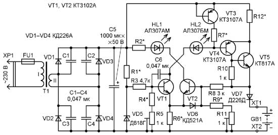
The power supply of the AZU from the network is carried out through a step-down transformer, which ensures electrical safety, followed by a rectifier bridge VD1 -VD4. If the AZU will be used to power the radio, then to eliminate the so-called multiplicative background, the diodes should be bridged with ceramic capacitors. Capacitor C1 smoothes the ripple of the rectified voltage, its capacitance should be at least 1000 μF for every 100 mA of current consumption. The reference voltage (9 V) is removed from the precision Zener diode VD5. Resistor R1 determines its rated stabilization current (10 mA). The voltage limitation on the battery (battery) upon reaching full charge is carried out by the differential cascade VT1VT2 as follows. The set voltage, at which it is necessary to limit the charging current, is determined by the voltage divider R2R3 and applied to the base of the transistor VT1, and the base VT2 receives voltage from the battery, taking into account the voltage drop across the diode VD7, which disconnects the battery from the battery when the voltage fails. Until the battery is charged, the voltage based on VT2 is less than that based on VT1, and therefore, VT2 is closed and the HL2 LED does not light. HL1 is on because VT1 is in active mode. The current value is determined by the resistance of the resistor R5 and the voltage based on VT1 and does not depend on the voltage on its collector. Such a circuit is known as a current source (IT) [2]. Consequently, the voltage drop across the resistor R4 will be stable, and HL1 will glow, indicating that the battery is charging. Its charging current is stable and does not depend on the voltage on the battery, since transistors VT3 and VT4 form IT.
Particular accuracy in maintaining the charging current is not required; limiting the battery voltage when reaching full charge is crucial. The accuracy of the differential stage and the parametric voltage regulator is quite enough to solve this problem. When the voltage on the battery corresponding to the full charge is reached, the transistor VT2 goes into active mode, its collector current appears, the HL2 LED lights up, indicating that the battery is charged, the current through VT1 will decrease, and the charge current will decrease to 0.01 ... 0.02Q, which eliminates battery recharging and damage. Capacitor C2 eliminates possible self-excitation, resistor R6 reduces the voltage across the VT2 collector, and therefore the power dissipated by it. The VD6 diode provides reliable closing of the VT4 transistor.

The VT4 transistor can be replaced by any of the KT973, KT814, KT816 series and others (taking into account the charging current and the power dissipated in this case), VT3 - by any transistor from the KT3102, KT315, KT503 series, and VT1, VT2 - by any of the KT203, KT208, KT209 series KT502. The current transfer coefficient of the base of transistors is not less than 50.
If you need to charge the battery with large capacities and (or) voltages, you can assemble the battery according to the scheme shown in Fig. 2, using transistors of a different structure as more common. An exemplary voltage and a comparison with it is supplied to the base of the transistors of the differential stage through dividers or directly, depending on the voltage of the battery. So, if its voltage is less than 9 V (stabilization voltage D818 = 9 V), then the resistors R9, R11 are excluded, the voltage is supplied to the VT2 base through the resistor R8, and the required value of the battery charging end voltage is set by the divider R3R4R5.


If the battery voltage is more than 9 V, then the resistors R4, R5 are excluded, and the charging end voltage is set by the divider R8R9R1 1. The current of the dividers is selected in the range of 0.5 ... 1 mA. The resistor R6 sets the charging current of about 10 mA after determining the voltage on the basis of the transistor VT1. By choosing a resistor R1, the nominal stabilization current of the Zener diode VD5 is set to 10 mA. The VD6 diode limits the reverse voltage at the VT2 emitter junction, which can occur during a short circuit in the battery circuit.
Transistors VT3, VT4, VT5 form a powerful current source [2]. Thanks to the first of them, the voltage drop across the resistors R7, R12 can be set on the order of 1 V, which may be required if the battery voltage is comparable with the voltage at the output of the rectifier. With a battery voltage of less than 9 V, the VT3 transistor can be excluded, and the voltage drop across the resistors R7, R12 should be selected equal to several volts, while the power dissipated by the transistor VT5 will decrease, but a resistor R12 with a correspondingly higher dissipation power will be required.
The power and voltage on the secondary winding of the step-down transformer T1, the electrical parameters of the diodes VD1-VD4, VD7, transistor VT5 are determined by the capacity and voltage of the battery. To ensure long trouble-free operation of the device, the limit values of the parameters of semiconductor devices and resistors must exceed the values existing in the device by 2 ... 3 times. If it is assumed that the device will work around the clock without supervision, special attention should be paid to fire safety. The transformer must be of sufficient power, with reliable insulation and low idle current, indicating the absence of saturation of the magnetic circuit and a sufficient number of turns of the primary winding. To determine the maximum permissible mains voltage and identify short-circuited turns it is useful to take off the magnetization characteristic of the transformer (the dependence of the open-circuit current on the voltage on the mains winding). A sharp increase in the open-circuit current is permissible only when the voltage on the winding exceeds the rated mains by 10% (with a nominal 230 V it is 253 V), which indicates a sufficient number of turns of the primary winding. The housing of the control unit must also meet the requirements of fire and electrical safety.
When setting up, the rectifier of the AZU should be loaded with a current of 0.01 ... 0.02 Q and the nominal charging current (approximately 10 mA) should be set by selecting resistor R6, since it is in this mode that the charging current should be limited. Then, depending on the voltage of the battery, select the configuration of the circuit of the device and pre-set the voltage limiting the charging of the battery. If this voltage is more than 9 V, then, according to the above, the base of the transistor VT1 is connected to the zener diode VD5 through the resistor R3, in this case the voltage on its emitter will be less than about 0.65 V, i.e. about 8.4 V. Therefore , at a current of about 10 mA, the nearest value of the resistor R6 is 820 Ohms. Then determine the values of the resistors R7, R12 and the need for a transistor VT3 to achieve the required charging current. When measuring the charging current, the HL1 LED should not light. To perform this work, the AZU is loaded with a chain according to the scheme in Fig. 3. Next, the tuning resistor R11 sets the current to 0.01 ... 0.2Q with a voltage at the output of the AZU corresponding to 1.5 V for each battery of the battery.

If the battery voltage is less than 9 V, then R9, R11 are excluded, using the dividers R3R4R5, the voltage corresponding to the charged battery plus the voltage drop across the VD7 diode is pre-set, then, according to the above, the resistance of the resistors R6, R7, R12 is determined and the charge limiting voltage is finally set Battery trimmer resistor R5.

Literature
 A little bit about charging nickel-cadmium batteries. - Radio, 1996, No. 7, p. 48.
 Semushin S. Sources of current and their application. - Radio, 1978, No. 1, p. 39; No. 2, p. 44.
Author: S. Tikhonov, the city of Kaltan, Kemerovo region


CHARGER FOR NI-MH BATTERY

The reason for the development and manufacture of the proposed device was the desire to replace the galvanic power element of the wall electromechanical clock with a battery. The available charger allowed charging only an even number of batteries, and one AA-size Ni-MH battery needed to be charged.
When viewing the literature, I was interested in “Automatic Battery Charger” described by N. Skrindevsky in Radio, 1991, No. 12, p. 28-30. I liked the idea embedded in this design to charge the battery cyclically, alternating charging intervals with intervals measuring the emf of the battery. As a result of prototyping and debugging, the proposed charger was obtained.
Key Specifications
Supply voltage, V ............. 5
Charging current, mA …………… ..150
The threshold for switching off the charging current, V ………………… 1.38
The threshold for switching on the charging current, V …………………… .. 1
The duration of the charging cycle, s .............................. 40
Duration of measurement, s ……… 1
A diagram of this device is shown in Fig. 1. A current source is assembled on the transistor VT2, resistors R9-R12 and LED HL1. It is controlled by transistor VT1. The HL1 LED has two functions: it serves as a source of stable voltage supplied to the base of transistor VT2 through resistor R10, and at the same time as a battery indicator. Resistors R11 and R12 set the charging current, the value of which in milliamperes is chosen numerically equal to the nominal battery capacity G1 in milliampere-hours. Resistor R9 limits the current through the LED HL1. The VD2 diode prevents the discharge of the G1 battery through the charger in the event of a power failure or a power outage.


On a voltage comparator DA1.1, resistors R1-R6, capacitor C1 and diode VD1, a pulse sequence generator with a duration of 40 s with a pause of 1 s is assembled. In the pauses between pulses, the EMF of the battery is measured.
During the measurement, the current source is disconnected from the rechargeable battery. At this time, the voltage on the battery is compared with the model voltage - the one to which the battery needs to be charged. The diode VD4 prevents the blocking voltage from reaching the engine trimmer resistor R14.
On the voltage comparator DA1.2 and resistors R13-R17, a Schmitt trigger is assembled, which controls the voltage on the rechargeable battery. For the trigger to work correctly, a blocking voltage is supplied to the inverting input of the comparator DA1.2 from the output of the comparator DA1.1 during charging through the VD3 diode.
Upon reaching the voltage on the battery set by the tuning resistor R14 and applied to the inverting input of the comparator DA1.2, a high level voltage appears at the output of the last one, which is fed through the diode VD5 to the inverting input of the comparator DA1. 1, blocking the operation of the generator. At the output of the comparator DA1.1, a low voltage level is set, the transistor VT1 closes, the LED HL1 goes out.
At the same time, a high level voltage from the output of the comparator DA1.2 is also supplied to the base of the transistor VT3, opening it, the HL2 LED turns on, signaling the completion of battery charging. The reference voltage at the inverting input of the comparator DA1.2 is chosen equal to 1.38 V - the same as that of an available industrial charger.
The LM393N chip can be replaced with K1401CA3A or another of its many analogues, and KT312V transistors can be replaced with similar ones with other letter indices or with KT315 series transistors. Replacement of the KT816V transistor can be the KT814V. Instead of D223 diodes, D220 or the KD522 series are suitable, and instead of KD226A, any rectifier diode with a permissible forward current of at least 200 mA is suitable. When replacing the AL307 series LEDs with more modern ones, it is recommended to increase the values of the resistors R9 and R20 in order to reduce the brightness of their glow to an acceptable level.

Oxide capacitors C1, C2 - imported or domestic series K50-16, K50-35. Capacitors C3 and C4 - any ceramic or film. Trimmer resistor R14 - imported. Fixed resistors - MLT-0.125 or similar.
The charger is assembled in a small housing from the dental handpiece. With the lid open, it is shown in fig. 2. Initially, it was planned to place the battery holder (contacts X1 and X2) directly on the printed circuit board, and the board was designed specifically for this location. Subsequently, the holder was glued into the housing cover.


The drawing of the circuit board of the charger is shown in Fig. 3. For the LM393N chip, a panel is installed on it. Permanent resistors are installed both parallel and perpendicular to the surface of the board. One of the pins of resistor R2 and pin
the cathode of the diode VD1 is soldered into the board, and the remaining free conclusions of these elements are connected above it. The battery holder and LEDs glued into the housing cover are connected to the board by flexible insulated mounting wires.


In a properly assembled device, you only need to adjust the battery charging current and charging disconnect voltage. Before setting the charging current, the DA1 chip must be removed from the panel, and instead of a battery, connect a 33 Ohm resistor or a miniature incandescent lamp MN 6.3-0.3 to the terminals X1 and X2 through a multimeter in the direct current measurement mode with a limit of at least 200 mA. A selection of resistors R11, R12 should set the multimeter to 150 mA. But you can set another charging current, depending on the capacity of the battery.
Adjusting the voltage to turn off the battery charging is reduced to setting the trimmer resistor R14 voltage of 1.38 V between sockets 2 and 4 of the comparator panel. After that, you need to disconnect the device from the power source and insert the chip into the panel. The charger is ready to use.
The width of the trigger hysteresis loop on the comparator DA1.2 depends on the ratio of the resistance of the resistors R15 and R16. Decreasing the resistance of resistor R15 increases the trigger voltage.

Author: G. Kosolapov, Kirovo-Chepetsk, Kirov Region

POWER SUPPLY 220V TO + 5 ... 15V / 20A

This power supply gives a voltage of 5 to 15V, stable installed in these limits, with a maximum current of 20A. At a current of more than 22A, protection is triggered.
AC voltage 220V from the mains is supplied through a 4-amp fuse F1 to the primary winding of the T1 power transformer. This is a ready-made transformer with a primary winding at 230V and secondary at 20V at a current of up to 20A. If necessary, such a transformer can be manufactured independently on the basis of a power transformer from an old color lamp television, or on the basis of a low-frequency power transformer with a power of at least 500W to power halogen lamps (12V), or to obtain 36V for powering equipment by rewinding its secondary winding accordingly.


From the secondary winding, a voltage of 20V is supplied to the rectifier bridge VD1. This is a finished bridge assembly type MB356, designed for a maximum DC current of 35A. The ripple of the rectified voltage is smoothed by a capacitor C1 with a capacity of 22,000 microfarads. In the absence of a capacitor of such a large capacitance, it can be replaced by several capacitors of a smaller capacity, connected in parallel, so that in total they give at least 20,000 μF.
The constant voltage at capacitor C1 at idle is 28V.
The stabilizer consists of a stabilizer circuit on the IC A1 and an output voltage regulator on transistors VT1-VT5, the powerful transistors VT2-VT5 of which are connected in parallel. Resistors R5-R8 are used to equalize the current through the transistors, as as a result of differences in the transmission coefficients, they can, under equal conditions, open to different degrees. The resistors included in the emitter circuits help automatically set the base-emitter voltages under the action of the load current, at which the transistors open equally.
The LM723 is an integrated stabilizer with adjustable output voltage and an overload protection circuit. The output voltage is regulated by the resistor R3, which, together with the resistors R2, forms the output voltage divider. By adjusting, the dependence of the voltage at terminal 4 A1 on the output voltage is established. The comparator of the microcircuit works so that the voltage at the output (terminal 10) is regulated so that the voltage at its output 4 is unchanged. Accordingly, the voltage at terminal 10 is almost equal to the output. But the maximum permissible output current is small, therefore, to obtain a maximum load current of 20A, a current amplifier is needed, which is a VT1-VT5 transistor circuit.

The overcurrent protection circuit works by measuring the voltage across a resistance connected in series with the load. The inputs of the current sensor are terminals 2 and 3 A1. These pins are connected in parallel with the resistance formed by the resistors R9-R12, which is connected in series with the load. It is clear that, following Ohm's law, the voltage across the resistance will increase with increasing current. While the voltage between pins 2 and 3 is lower than 0.6V, the protection does not work, perceiving this as the fact that the load current does not exceed the maximum permissible value. At a current approaching the level of 22-23 A, the voltage between terminals 2 and 3 reaches a value of 0.6V or more. This leads to the operation of the protection, which reduces the voltage at terminal 10 A1 to zero, and thus disconnects the load.

The maximum output current can be set by another, accordingly changing the resulting resistance R9-R12, which in this case, provided that the upper threshold of the load current 23A is selected, is 0.025 Ohm. Or you can even organize the adjustment of the maximum output current if you turn on one low-resistance resistor R9-R12 with one variable resistor, somewhere around 10-100 Ohms, and remove the control voltage from its engine and one of the extreme terminals. The resistor will be a voltage divider on R9-R12. But in this case, the resistance R9-R12 must be calculated on the lower limit of the adjustment of the maximum load current.
The circuit provides a fairly good stability of the installed output voltage, for example, with an output voltage of 13V, under a load of 20A, the voltage decreases by only 40-60 mV.
LED HL1 is used to indicate the status connected to the network. The HL2 LED indicates the normal output mode of the power supply. That is, it burns when there is voltage at the output. If it is not lit, but HL1 is lit, this indicates that there is a short circuit on the load or overload and the stabilizer output is turned off by the current protection system, or that the fuse F2 is turned on at the output of the rectifier.
Transistors VT2-VT5 must be on volumetric radiators, ensuring their effective cooling. A good option is to use a plate aluminum radiator with a fan. In this case, the radiator and fan can be used from a faulty power supply of a personal computer of the AT or ATX type. The fan motor can be connected in parallel to the capacitor C1 through a resistor, which reduces the voltage on the fan to 12V.
Details The transformer is said at the beginning of the article. Capacitor C1 is an analogue of K50-35, imported, at 22,000 microfarads. Can be replaced by several capacitors of lower capacitance, connected in parallel, in the amount of not less than 20,000 μF.

The rectifier bridge can be replaced by another with a direct current of at least 30A, or assemble it on diodes designed for the same current, for example, 2D2997, KD2997, KD2998.
Transistors 1N3055 can be replaced by KT819. It is necessary to take transistors as close as possible in parameters. It is advisable, with one letter designation, from the same batch, and even better, before installation, select them according to the closest possible coefficients h21e.
LEDs - ordinary, indicator, almost any. You can use AL307. With insufficient brightness, the resistance of the resistors R1 and R13 can be reduced.
Resistors R5-R12 - five-watt, wire, resistance 0.1 Ohm.
If a pointer millivoltmeter is connected in parallel with resistors R9-R12, then on its scale it will be possible to determine the load current (accordingly, by redoing its scale in units of current strength).

Author: Gorchuk N.V.


Monday, 10 February 2020

200 WATT AUDIO AMPLIFIER CIRCUIT DIAGRAM

  200 WATT AUDIO AMPLIFIER

Diagram 200 WATT AUDIO AMPLIFIER
Output Power : 200Watts
Load Resistance : 8ohms
Input impedance : 55K
Maximum supply voltage : (+95v)-0-(-95v)
Recommended supply voltage : (+66v)-0-(-66v)


This complete high quality, low noise mono audio power amplifier is based around the Hybrid Integrated Circuit STK4050 manufactured by Sanyo. The circuit incorporates volume and has a maximum music output power of 200W. The circuit incorporates an on board power supply; therefore, only centre tapped transformer is required to power the circuit. I t has very good quality sound. U can use it with your Home Theatre your PC & etc... You can also use it as Subwoofer Amplifier. It is a compact package for THIN-TYPE Audio sets. Easy Heat sink design to disperse heat generated in THIN-TYPE audio sets. Constant-Current circuit to Reduce supply switch-ON and switch-OFF shock noise. External supply switch-On and switch-OFF shock noise muting, Load short-circuit protection, thermal shutdown and other circuits can be tailored-designed.