LOEWE Spheres R 32 HD - Power supply schematic diagram - l6599 - MC33262 - LCD TV Repair and service - Tips Manual
Category: LCD Power Supply Repair and Service
Contents of this article
- MC33262 Power factor controller
- L6599 smps driver
- Power supply Schematic diagram
LOEWE Spheres R 32 HD
MC33262 Power Factor Controllers
Description
The MC34262/MC33262 are active power factor controllers specifically designed
for use as a preconverter in electronic ballast and in off–line power converter
applications. These integrated circuits feature an internal startup timer for
stand–alone applications, a one quadrant multiplier for near unity power
factor, zero current detector to ensure critical conduction operation,
transconductance error amplifier, quickstart circuit for enhanced startup,
trimmed internal bandgap reference, current sensing comparator, and a totem pole
output ideally suited for driving a power MOSFET. Also included are protective
features consisting of an overvoltage comparator to eliminate runaway output
voltage due to load removal, input under voltage lockout with hysteresis,
cycle–by–cycle current limiting, multiplier output clamp that limits maximum
peak switch current, an RS latch for single pulse metering, and a drive output
high state clamp for MOSFET gate protection. These devices are available in
dual–in–line and surface mount plastic packages.
FEATURES
Overvoltage Comparator Eliminates Runaway
Output Voltage
Internal Startup Timer
One Quadrant Multiplier
Zero Current Detector
Trimmed 2% Internal Bandgap Reference
Totem Pole Output with High State Clamp
Undervoltage Lockout with 6.0 V of Hysteresis
Low Startup and Operating Current
Supersedes Functionality of SG3561 and TDA4817
L6599
Description
The L6599 is a double-ended controller specific for the resonant half-bridge
topology. It provides 50 % complementary duty cycle: the high-side switch and
the low-side switch are driven ON\OFF 180° out-of-phase for exactly the same
time. Output voltage regulation is obtained by modulating the operating
frequency. A fixed deadtime inserted between the turn-OFF of one switch and the
turn-ON of the other one guarantees soft-switching and enables high-frequency
operation.
To drive the high-side switch with the bootstrap approach, the IC incorporates
a high-voltage floating structure able to withstand more than 600 V with a
synchronous-driven high-voltage DMOS that replaces the external fast-recovery
bootstrap diode. The IC enables the designer to set the operating frequency
range of the converter by means of an externally programmable oscillator.
At start-up, to prevent uncontrolled inrush current, the switching frequency
starts from a programmable maximum value and progressively decays until it
reaches the steady-state value determined by the control loop. This frequency
shift is non linear to minimize output voltage overshoots; its duration is
programmable as well. The IC can be forced to enter a controlled burst-mode
operation at light load, so as to keep converter's input consumption to a
minimum. IC's functions include a not-latched active-low disable input with
current hysteresis useful for power sequencing or for brownout protection, a
current sense input for OCP with frequency shift and delayed shutdown with automatic
restart. A higher level OCP latches off the IC if the first-level protection is
not sufficient to control the primary current. Their combination offers
complete protection against overload and short circuits. An additional latched
disable input (DIS) allows easy implementation of OTP and/or OVP.
An interface with the PFC controller is provided that enables to switch off the
pre-regulator during fault conditions, such as OCP shutdown and DIS high, or
during burst-mode operation.
PIN CONFIGURATION
1 C SS
Soft start. This pin connects an external capacitor to GND and a resistor to
RFmin (pin 4) that set both the maximum oscillator frequency and the time
constant for the frequency shift that occurs as the chip starts up
(soft-start). An internal switch discharges this capacitor every time the chip
turns OFF (VCC < UVLO, LINE < 1.25 V or > 6 V, DIS > 1.85 V, ISEN
> 1.5 V, DELAY > 3.5 V) to make sure it will be soft-started next, and
when the voltage on the current sense pin (ISEN) exceeds 0.8V, as long as it
stays above 0.75 V.
2 DELAY
Delayed shutdown upon overcurrent. A capacitor and a resistor are connected
from this pin to GND to set both the maximum duration of an overcurrent
condition before the IC stops switching and the delay after which the IC restarts
switching. Every time the voltage on the ISEN pin exceeds 0.8 V the capacitor
is charged by an internal 150µA current generator and is slowly discharged by
the external resistor. If the voltage on the pin reaches 2 V, the soft start
capacitor is completely discharged so that the switching frequency is pushed to
its maximum value and the 150 µA is kept always on. As the voltage on the pin
exceeds 3.5 V the IC stops switching and the internal generator is turned OFF,
so that the voltage on the pin will decay because of the external resistor. The
IC will be soft-restarted as the voltage drops below 0.3V. In this way, under
short circuit conditions, the converter will work intermittently with very low
input average power.
3 CF
Timing capacitor. A capacitor connected from this pin to GND is charged and
discharged by internal current generators programmed by the external network
connected to pin 4 (RFmin) and determines the switching frequency of the
converter.
4 RFmin
Minimum oscillator frequency setting. This pin provides a precise 2 V reference
and a resistor connected from this pin to GND defines a current that is used to
set the minimum oscillator frequency. To close the feedback loop that regulates
the converter output voltage by modulating the oscillator frequency, the
phototransistor of an optocoupler will be connected to this pin through a
resistor. The value of this resistor will set the maximum operating frequency.
An R-C series connected from this pin to GND sets frequency shift at start-up
to prevent excessive energy inrush (soft-start).
5 STBY
Burst-mode operation threshold. The pin senses some voltage related to the
feedback control, which is compared to an internal reference (1.25 V). If the
voltage on the pin is lower than the reference, the IC enters an idle state and
its quiescent current is reduced. The chip restarts switching as the voltage
exceeds the reference by 50 mV. Soft-start is not invoked. This function
realizes burst-mode operation when the load falls below a level that can be
programmed by properly choosing the resistor connecting the optocoupler to pin
RFmin (see block diagram). Tie the pin to RFmin if burst-mode is not used.
6 ISEN
Current sense input. The pin senses the primary current though a sense resistor
or a capacitive divider for lossless sensing. This input is not intended for a
cycle-by-cycle control; hence the voltage signal must be filtered to get
average current information. As the voltage exceeds a 0.8 V threshold (with 50
mV hysteresis), the soft-start capacitor connected to pin 1 is internally
discharged: the frequency increases hence limiting the power throughput. Under
output short circuit, this normally results in a nearly constant peak primary
current. This condition is allowed for a maximum time set at pin 2. If the
current keeps on building up despite this frequency increase, a second
comparator referenced at 1.5 V latches the device off and brings its
consumption almost to a “before start-up” level. The information is latched and
it is necessary to recycle the supply voltage of the IC to enable it to
restart: the latch is removed as the voltage on the Vcc pin goes below the UVLO
threshold. Tie the pin to GND if the function is not used.
7 LINE
Line sensing input. The pin is to be connected to the high-voltage input bus
with a resistor divider to perform either AC or DC (in systems with PFC)
brownout protection. A voltage below 1.25 V shuts down (not latched) the IC,
lowers its consumption and discharges the soft-start capacitor. IC’s operation
is re-enabled (soft-started) as the voltage exceeds 1.25 V. The comparator is
provided with current hysteresis: an internal 15 µA current generator is ON as
long as the voltage applied at the pin is below 1.25 V and is OFF if this value
is exceeded. Bypass the pin with a capacitor to GND to reduce noise pick-up.
The voltage on the pin is top-limited by an internal zener. Activating the
zener causes the IC to shut down (not latched). Bias the pin between 1.25 and 6
V if the function is not used.
8 DIS
Latched device shutdown. Internally the pin connects a comparator that, when
the voltage on the pin exceeds 1.85 V, shuts the IC down and brings its
consumption almost to a “before start-up” level. The information is latched and
it is necessary to recycle the supply voltage of the IC to enable it to
restart: the latch is removed as the voltage on the VCC pin goes below the UVLO
threshold. Tie the pin to GND if the function is not used.
9 PFC_STOP
Open-drain ON/OFF control of PFC controller. This pin, normally open, is
intended for stopping the PFC controller, for protection purpose or during
burst-mode operation. It goes low when the IC is shut down by DIS > 1.85 V,
ISEN > 1.5 V, LINE > 6 V and STBY < 1.25 V. The pin is pulled low also
when the voltage on pin DELAY exceeds 2V and goes back open as the voltage
falls below 0.3V. During UVLO, it is open. Leave the pin unconnected if not
used.
10 GND
Chip ground. Current return for both the low-side gate-drive current and the
bias current of the IC. All of the ground connections of the bias components
should be tied to a track going to this pin and kept separate from any pulsed
current return.
11 LVG
Low-side gate-drive output. The driver is capable of 0.3 A min. source and 0.8
A min. sink peak current to drive the lower MOSFET of the half-bridge leg. The
pin is actively pulled to GND during UVLO.
12 VCC
Supply Voltage of both the signal part of the IC and the low-side gate driver.
Sometimes a small bypass capacitor (0.1 µF typ.) to GND might be useful to get
a clean bias voltage for the signal part of the IC.
13 N.C.
High-voltage spacer. The pin is not
internally connected to isolate the high-voltage pin and ease compliance with
safety regulations (creepage distance) on the PCB.
14 OUT
High-side gate-drive floating ground. Current
return for the high-side gate-drive current. Layout carefully the connection of
this pin to avoid too large spikes below ground.
15 HVG
High-side floating gate-drive output. The driver is capable of 0.3 A min.
source and 0.8A min. sink peak current to drive the upper MOSFET of the
half-bridge leg. A resistor internally connected to pin 14 (OUT) ensures that
the pin is not floating during UVLO.
16 VBOOT
High-side gate-drive floating supply Voltage. The bootstrap capacitor connected
between this pin and pin 14 (OUT) is fed by an internal synchronous bootstrap
diode driven in-phase with the low-side gate-drive. This patented structure
replaces the normally used external diode.
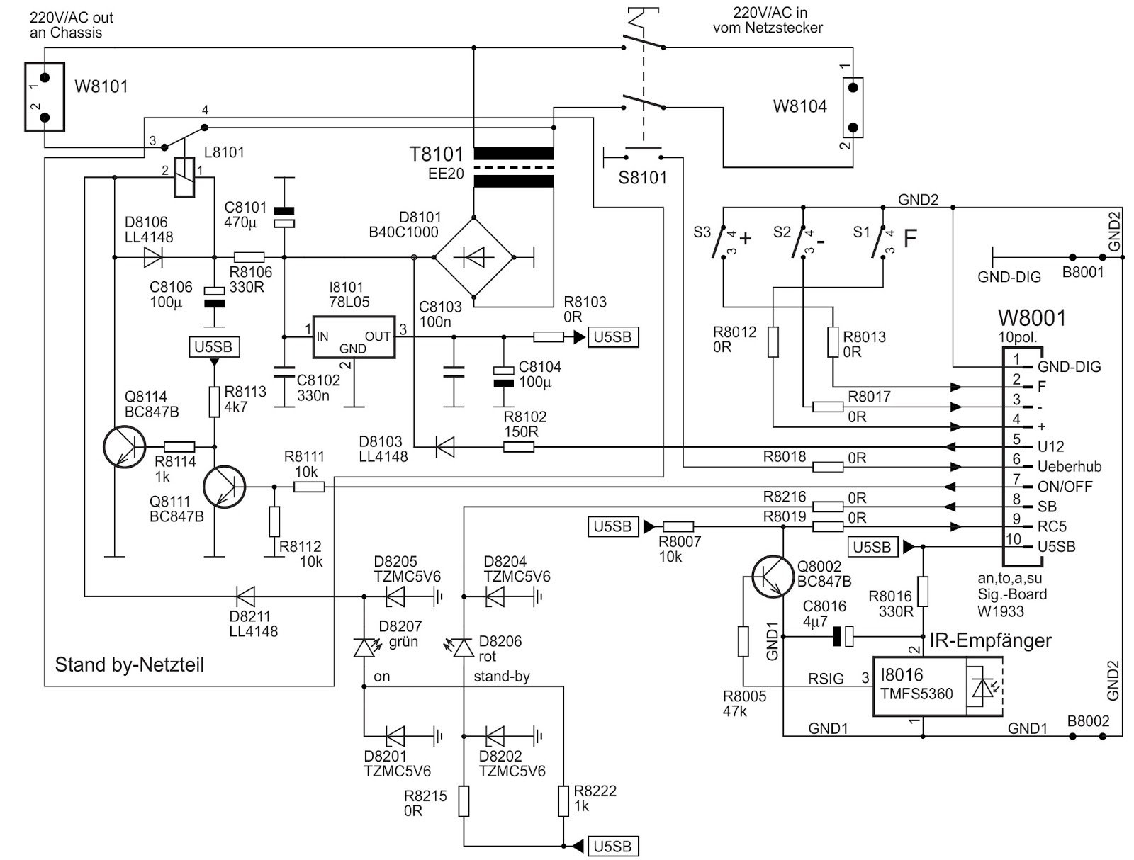
POWER SUPPLY SCHEMATIC DIAGRAM
CLICK ON THE IMAGE TO ZOOM IN

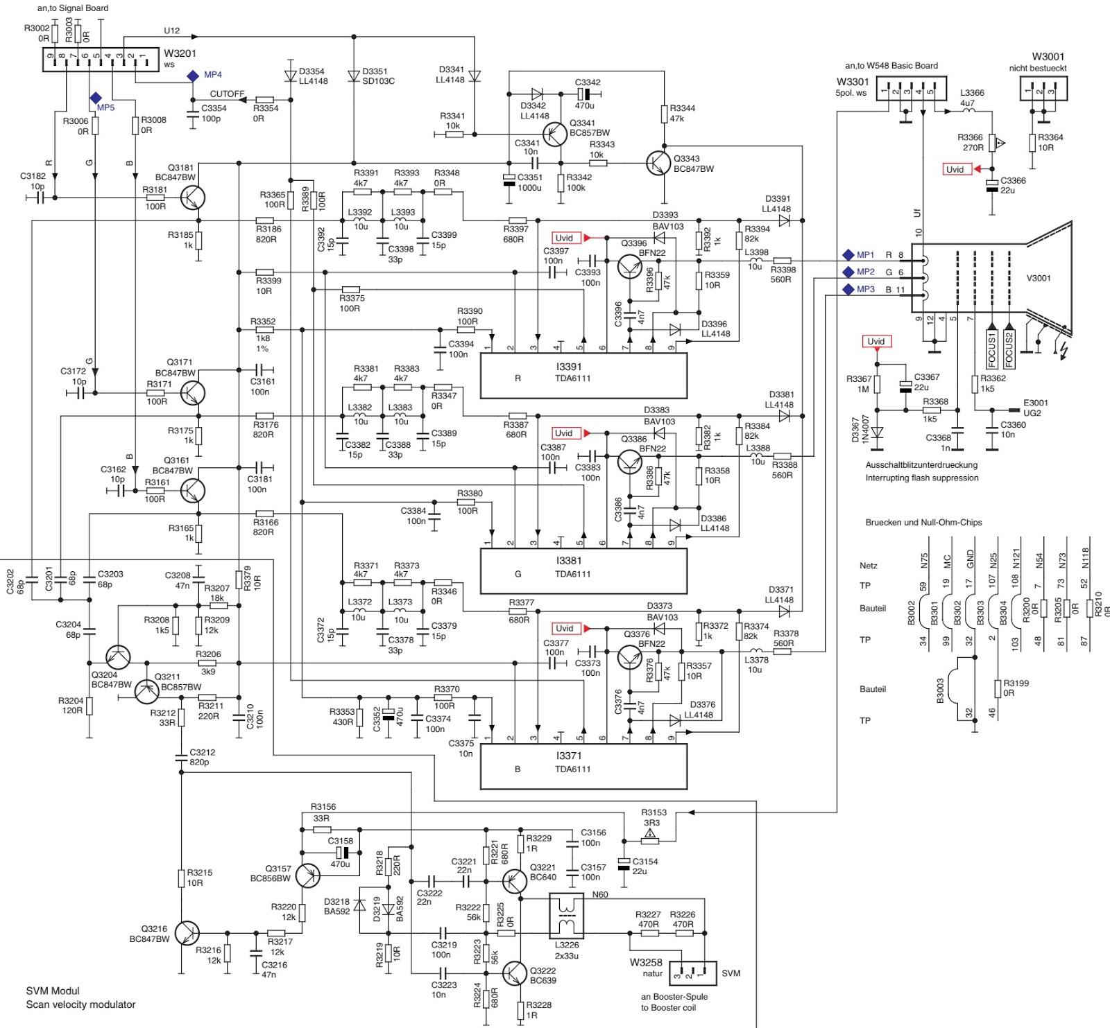
 Loewe CRT TV - Circuit Diagram