REPAIRING AND NOT THROWING AWAY

Richtige Fernseher haben Röhren!

Richtige Fernseher haben Röhren!

In Brief: On this site you will find pictures and technical information about Service Modes, Circuit Diagrams, Firmware Update procedure, Disassemble procedure, Universal remote control set-up codes, Troubleshooting and more....

If you go into the profession, you will obtain or have access to a variety of tech tips databases HERE IT IS Master Electronics Repair !.

These are an excellent investment where the saying: 'time-is-money' rules. However, to learn, you need to develop a general troubleshooting approach - a logical, methodical, method of narrowing down the problem. A tech tip database might suggest: 'Replace C536' for a particular symptom. This is good advice for a specific problem on one model. However, what you really want to understand is why C536 was the cause and how to pinpoint the culprit in general even if you don't have a service manual or schematic and your tech tip database doesn't have an entry for your sick TV or VCR.

While schematics are nice, you won't always have them or be able to justify the purchase for a one-of repair. Therefore, in many cases, some reverse engineering will be necessary. The time will be well spent since even if you don't see another instance of the same model in your entire lifetime, you will have learned something in the process that can be applied to other equipment problems.
As always, when you get stuck, checking out a tech-tips database may quickly identify your problem and solution.In that case, you can greatly simplify your troubleshooting or at least confirm a diagnosis before ordering parts.

Happy repairing!
Today, the West is headed for the abyss. For the ultimate fate of our disposable society is for that society itself to be disposed of. And this will happen sooner, rather than later.

How to use the site:

- If you landed here via any Search Engine, you will get what you searched for and you can search more using the search this blog feature provided by Google. You can visit more posts scrolling the left blog archive of all posts of the month/year,
or you can click on the main photo-page to start from the main page. Doing so it starts from the most recent post to the older post simple clicking on the Older Post button on the bottom of each page after reading , post after post.

You can even visit all posts, time to time, when reaching the bottom end of each page and click on the Older Post button.

- If you arrived here at the main page via bookmark you can visit all the site scrolling the left blog archive of all posts of the month/year pointing were you want , or more simple You can even visit all blog posts, from newer to older, clicking at the end of each bottom page on the Older Post button.
So you can see all the blog/site content surfing all pages in it.

- The search this blog feature provided by Google is a real search engine. If you're pointing particular things it will search IT for you; or you can place a brand name in the search query at your choice and visit all results page by page. It's useful since the content of the site is very large.

Note that if you don't find what you searched for, try it after a period of time; the site is a never ending job !

..............The bitterness of poor quality is remembered long after the sweetness of todays funny gadgets low price has faded from memory........ . . . . . .....
Don't forget the past, the end of the world is upon us! Pretty soon it will all turn to dust!

©2010, 2011, 2012, 2013, 2014 Frank Sharp - You do not have permission to copy photos and words from this blog, and any content may be never used it for auctions or commercial purposes, however feel free to post anything you see here with a courtesy link back, btw a link to the original post here , is mandatory.
All posts are presented here for informative, historical and educative purposes as applicable within fair use. NOTHING HERE IS FOR SALE !

Showing posts with label PSU. Show all posts

Friday, 1 March 2019

VESTEL 17IPS20 POWER BOARD CIRCUIT DIAGRAM – USED WITH TOSHIBA LCD TV LT-40DG51J

Vestel 17IPS20 Power Board Circuit Diagram – Used with Toshiba LCD TV LT-40DG51J


Vestel 17IPS20P: Used ICs FAN7529 – SG6742HR – CAP002DG – FQPF9N50C (FET) – M3394 

Circuit Diagram


Click on the schematics to magnify

Friday, 8 February 2019

SONY WEGA SERIES TVS – POWER SUPPLY FAULTS

SONY WEGA SERIES TVs – POWER SUPPLY FAULTS

KV-HA21M50_ KV-HA21M80_ KV-HA21M80/H_ KV-HA21M81_ KV-HA21P52_ KV-HA14M80 & KV-HW21M83 : POWER SUPPLY FAULTS
Cont:-
Section –2

       We have already reached half the way by troubleshooting power supply section.  We have found that here is no fault with mains ON/OFF switch, Rectifier Bridge, switching regulator IC, posistor.  The main component to check further is (R610 – 33Kohms 3W) resistor, which supplies voltage to the internal circuits of the switching IC.  This is one among the important test point.  Check the voltage at (Pin-4) of regulator IC.  If there is no voltage, check this resistor for open.  If it is found OK, check the zener diode (D603) for short.  Replace it, it is best.  If switching regulator IC found shorted, you have to check all the components on the primary side of the SMPS power supply.  Even a small ceramic capacitor can cause severe trouble to switching power section.

      It is recommended to use a 100W filament type bulb at the secondary [135] VDC line, after disconnecting (R502), the serial resistor connected to LOT power supply.  You can reconnect this after finishing the power supply work. When a set comes to you for repair, with dead power regulator section, with shorted switching IC [STR F6707A], be very careful, and check all other components, for any short, open or any other trouble.  Replace these components, even if they are found good. [C610, D605, R608, R605, D603&C606]. If power regulation is found poor, check and replace (IC602 – SE135N) and optocoupler (PH600).  If STR are is found shorted, you have to replace all the above mentioned components, otherwise the newly replaced STR may get fail, as soon as you switch ON the set. 
Check all the solder terminals of SMPS transformer, and other components for loose soldering.  This is the main fault for most of the Sony set.  Resolder all the suspected solder points by applying a little more solder, without making any solder bridge short in between adjacent solder points.
 
C 623 & C 602 are very important capacitors, even though they are very small.  Replace both of them with same value

Thursday, 7 February 2019

PHILIPS 30 INCH AND 32 INCH LCD TV – POWER SUPPLY REGULATOR BOARD [SMPS] – SCHEMATIC

Philips 30 inch and 32 inch LCD TV – Power supply Regulator board [SMPS] – Schematic


Main Supply (Block "D")
Diversity
Mains input voltage diversity (1308):
– EU: 198 - 264 V AC.
– US: 108 - 132 V AC (doublers).
– AP multi: 90 - 275 V
AC (auto doubler with AVS10 control IC and triac).
– China: 160 - 270 V AC.
Mains filter diversity:
– EU, China: 1 x mains filter + harmonic coil.
– US, AP: 2 x mains filter + inrush current resistor.
Screen size diversity:
– One module for 30" to 37" sets.
– Two (almost identical) modules on one PWB for 42" sets.
Specifications
• 12 V / 3 A on connector 1304 (for Ambient Light and to generate +8V6).
• 24 V / 5 A for LCD back-light on connector 1304 (for Sharp 12 V, 9 A).
• +18V, -18V sound on connector 1M02.
• +8V6 (derived from +12V from the Main Supply, switched "off" in Stand-by).
• Output voltage: over-voltage protection of resonant supply.
• Output current protection of resonant supply.
• Current protection at some safety fault conditions.
Stand-by mode
• The resonant supply is switched "off" via relay 1450 that is driven by the Stand-by Supply (via connector 1305).
Outputs
• 130-400 V
DC (full range) for Stand-by Supply (connector 1306).
• Mains over-voltage and safety protection for Stand-by Supply (connector 1307).
Inputs
• Relay drive voltage (for STAND-BY/ON mode) on connector 1305.
• DC_PROT signal to protect loudspeakers when there is a DC voltage across the loudspeakers (1M02).


Stand-by Supply (Block "E")
The Stand-by Supply is based upon the "Fly Back Converter" principle. 

715G5793 - PHILIPS LED LCD TV - SMPS - CIRCUIT DIAGRAM

715G5793 - Philips LED LCD TV - SMPS - Circuit Diagram

Philips LED LCD TV power supply schematic 
ICs Used: PF7900S – PF7700A – PF622 – CAP004DG-TL – PF8200S – NR111D - STF10N65K3(FET) 
SMPS & LED back-light inverter schematic
Printed Circuit Board - Top & Foil side
CLICK ON THE PICTURES TO MAGNIFY

LG LIPS37 – LCD TV SMPS – SCHEMATIC

LG LIPS37 – LCD TV SMPS – Schematic


ICs Used: FA5501AN-TE1 – 3B1565J – AU3037 – FAN7601MX – FAN7382MX – KIA393F – LX1691AIPW – SPA04B60(FET)
Click on the schematics to zoom in

PHILIPS 32ME303V - MAGNAVOX 32 INCH LCD TV – FIRMWARE UPDATE – INITIALIZATION – SMPS SCHEMATIC BA3AF0F0102

Philips 32ME303V - MAGNAVOX 32 inch LCD TV – Firmware update – initialization – SMPS schematic BA3AF0F0102

HOW TO INITIALIZE THE LCD TV
The purpose of initialization is to place the set in a new out of box condition. The customer will be prompted to select a language and program channels after the set has been initialized.
To put the program back at the factory-default, initialize the LCD TV using the following procedure.
NOTE: Disconnect any device from the USB Port before you conduct on this procedure.
1. Turn the power on.
2. Enter the service mode.  To cancel the service mode, press [Power] button on the remote control unit.
3. Press [BACK] button to enter the Control Panel Key Confirmation Menu.
4. Press any button on the control panel.
5. Press [INFO] button to proceed with the self check mode.
6. Make sure to confirm the “INITIALIZED FINISH” appears in the green screen.
7. Unplug the AC Cord and plug it back on again.
Power supply Regulator [SMPS] - Circuit Diagram
Fixed voltage (or Auto voltage selectable) power supply circuit is used in this unit.  If Main Fuse (F602) is blown , check to see that all components in the power supply circuit are not defective before you connect the AC plug to the AC power supply.  Otherwise it may cause some components in the power supply circuit to fail.
For continued protection against risk of fire, replace only with same type 2.5A, 250V fuse.
Because a hot chassis ground is present in the power supply circuit, an isolation transformer must be used when repairing.  Also, in order to have the ability to increase the input slowly, when troubleshooting this type of power supply circuit, a variable isolation transformer is required.
The voltage for parts in hot circuit is measured using hot GND as a common terminal.
PWB - component and foil side
Firmware Update Procedure
User Upgrade (Filename example: TVNB012_00_UF_XX91_AC.ecc)
Upgrade the firmware only. The setting values will not be initialized.
The User Upgrade and the Firmware Upgrade (Factory Upgrade) will be done by the same file. If you want to upgrade the firmware and initialize the setting values also, add “FACT_” at the beginning of the filename.  If you want to upgrade the firmware only and leave the setting values as they are, eliminate the “FACT_” from the filename.
Update procedure
1. Turn the power on.
2. Press [MENU] button to display Menu.
3. Select “Features”.
4. Select “Software Upgrade”.
5. Select “Upgrade” to display Upgrade screen.
6. Press [OK] button to display Software Upgrade screen.
7. Select “USB” and press [OK] button.
8. Insert the USB storage device to the USB port.
9. Select “Check” and press [OK] button.
10. Select “Upgrade” and press [OK] button to start software upgrade.
11. The update will start and the following will appear in the screen.
12. When the firmware update is completed, will appear in the screen.
Factory Upgrade (Firmware Upgrade/Flash Upgrade)
Firmware Upgrade
(Filename example: FACT_TVNB012_00_UF_XX91_AC.ecc)
Upgrade the firmware and initialize the setting values.
The User Upgrade and the Firmware Upgrade (Factory Upgrade) will be done by the same file. If you want to upgrade the firmware and initialize the setting values also, add “FACT_” at the beginning of the filename.If you want to upgrade the firmware only and leave the setting values as they are, eliminate the “FACT_” from the filename.
Flash Upgrade
(Filename example: ALL_TVNB012_00_UF_XX91_AC.ecc)
Upgrade the firmware and initialize the setting values along with the factory default such as White Balance, etc.
Before the upgrade, you will need to make a note of all the factory default so you will be able to set it back on the TV after the initialization.
The Flash Upgrade will be done by its unique file.
The User Upgrade/Firmware Upgrade (Factory Upgrade) file cannot be used for this upgrade.
1.Turn the power off.
2. Insert the USB storage device to the USB port.
3. Turn the power on.
4. The update will start and the status will indicate in screen.
5. When the firmware update is completed, then the status will indicate in screen.
Remove the USB storage device from the USB port.
Turn the power off and turn the power on again.
Service mode initial screen with a word “INITIALIZED” will appear in the screen. The color of the word “INITIALIZED” will change from red to green when initialization is completed.

PHILIPS PLASMA TV FM23 - POWER AND AUDIO AMPLIFIER CIRCUIT DIAGRAM

Philips Plasma TV FM23 - Power and Audio amplifier Circuit Diagram


Audio Amplifier and Fan control Schematic
DC protection
Power Supply (SMPS) schematic

Click on the schematics TO ENLARGE.

Wednesday, 6 February 2019

PHILIPS AND HAIER LCD TV – SMPS SCHEMATIC (CIRCUIT DIAGRAM) - TEA1611T – MIP2F30MSSCF – UCC28061DR – STR G6153T

Philips and Haier LCD TV – SMPS Schematic (Circuit Diagram) - TEA1611T – MIP2F30MSSCF – UCC28061DR – STR G6153T

Philips 46PFL5706 - 46 inch LCD TV and Haier LCD TV – Power supply Schematic. Used ICs: TEA1611T – MIP2F30MSSCF – UCC28061DR – STR G6153T
Philips SMPS
Haier SMPS

Click on the schematics to zoom in

SANYO LCD 47XR8DA – HOW TO ENTER SERVICE MODE – ADJUSTMENT PROCEDURE

Sanyo LCD 47XR8DA – How to enter service mode – adjustment procedure – 


Adjustment instructions - How to enter Service Mode - SMPS schematic
Unit adjustments
1Connect all the boards according to wiring diagram, then power on and observe the display.
2 Method for entering factory menu:
a) Press “SOURCE”, “2”, “5”, ”8” and “0” in turn to enter factory menu;
b) Press “CH+” and “CH-” to move the cursor to the adjustment page of the level one factory menu, then press ”OK” to enter;
c) Press “CH+” and “CH-” to move the cursor up and down;
d) Press “VOL-” and “VOL+” to adjust the item when the cursor move to a certain adjust item;
e) Press “MENU” to exit to the previous factory menu;
f) Press “EXIT” to exit the factory menu at any situation;
g) Press “OK” to enter the sub factory menu;
h) ADC ADJUST, ADC correction of VGA, Component channel;
i) W/B ADJUST, white balance adjustment;
j) POWER Mode, set the turn-on modes. Standby---standby when power on; Mem---memory; ForceOn---power on; ForceOn can be used for aging; set the “power mode” to “Standby” when preset ex-factory unless the client appointed it;
k) ISP Mode, ON---soft upgrading through VGA port with ISP device, OFF---DDC function of VGA; the setting will not be memory and will be “OFF” when power on again;
l) REST ALL, initialization of the factory and user data; after this item is confirm, the unit will restart and display the guiding image.
m) Factory Data Reset, factory data initialization (including white balance adjustment, ADC correction and other adjusted data);
n) Factory Channel Preset, preset the factory channel; please connect to the center signal source when operating; the present digital frequency is CH28 (529.5MHz), CH33 (564.5MHz) for Australia and CH45 (666MHz) for UK, if the signal changes, perform “DTV manual search” in “Channel” menu and the operation needs 15s or so.
o) MST Debug, the default is OFF. OFF---RS-232 should match the design criterion; ON--- it should be convenient for using exploitation tool to adjust. The setting will not be memory and will be “OFF” when power on again;
p) Backlight: adjust the backlight brightness, adjust the data and test the voltage of X804 pin2 (PWM), let the voltage to be the corresponding PWM voltage which the brightness is maximum. It will be preset and doesn’t need adjust.
q) SSC Adjust, adjust the frequency spectrum expand, it will be preset and doesn’t need adjust.
r) AUDIO Curve, adjust the sound curve, it will be preset and doesn’t need adjust.
s) Picture Mode, set the picture values of each channel. Normally, they are preset and needn’t adjust.
t) There is data in EEPROM after software upgrade, please perform Reset All before the first adjustment.
ADC correction in VGA channel
a) Switch to VGA channel.
b) Press” SOURCE”, then press “2, 5, 8, 0” in turn to enter the level one factory menu.
c) Move the cursor to “ADC ADJUST” and press OK to enter the sub-menu.
d) Input VGA signal (VG-848 Timing:856(1024x768/60Hz), Pattern:920 Gray 8 step(H)). Move the cursor to “mode”, press CH+ and CH- to select “RGB”, move the cursor to “AUTO ADC” and press OK to adjust automatically till complete
ADC correction in YPbPr channel
a) Switch to YPbPr channel.
b) Press” SOURCE”, then press “2, 5, 8, 0” in turn to enter the level one factory menu.
c) Move the cursor to “ADC ADJUST” and press OK to enter the sub-menu.
d) Input YPbPr signal (VG-848 Timing:978(483P), Pattern:984 SMPTE Color Bar). Move the cursor to “mode”, press CH+ and CH- to select “YPbPr(HD)”, move the cursor to “AUTO ADC” and press ENTER to adjust automatically till complete.
e) Input YPbPr signal (VG-848 Timing:978(483P), Pattern:984 SMPTE Color Bar). Move the cursor to “mode”, press CH+ and CH- to select “YPbPr(SD)”, move the cursor to “AUTO ADC” and press ENTER to adjust automatically till complete.
White balance adjustment
The default of color temperature of COOL is 12000K and the coordinate is (272, 278); color temperature of NORMAL is 9300K and the coordinate is (285,293), color temperature of WARM is 6500K and the coordinate is (313,329).
Adjustment steps
Before the white balance adjustment, please let the unit working at least 30 minutes and at a stable situation, use BBY channel of the white balancer CA-210.
a) Switch to HDMI channel;
b) Press” SOURCE”, then press “2, 5, 8, 0” in turn to enter the level one factory menu.
c) Move the cursor to “W/B ADJUST” and press OK to enter the sub-menu.
d) Input DVI/HDMI signal 1024X768/60Hz 16 step Gray (Timing:856, Pattern:921). Move the cursor to “MODE”, press CH+ and CH- to select “HDMI” or other HDMI channel, move the cursor to “TEMPERTURE” and press CH+ and CH- to select “COOL”.
e) Fix G GAIN, adjust R GAIN, B GAIN and let the color coordinate of the fourteenth scale be (272,278).
f) Fix G OFFSET, adjust R OFFSET, B OFFSET and let the color coordinate of the third scale be (272,278).
g) When adjusting, please keep the color temperature of high light to be X=272±5, Y=278±5 and the low light to be X=272±8, Y=278±8.
h) Move the cursor to “COPY ALL” and copy the data to the other channels.
i) Check if the color temperatures of NORMAL and WARM are up to the mustard (low light acceptable error:±8, high light acceptable error:±5), if not, adjust R-GAIN/ B-GAIN/ R-OFF/ B-OFF.
j) Check the color temperature of COOL, NORMAL and WARM of other channels (ANALOGTV, DVB-T, Video, YPbPr,VGA), if they are not up to the mustard then adjust and store the data separately.
k) The reference of adjustment rule is below:
B gun: lower B gun to increase X, Y coordinate data, while raise B gun to decrease the data.
R gun: raise R gun to increase X coordinate data, while lower R gun to decrease the data; (R gun adjustment will affect X and Lv slightly).
G gun: raise G gun to increase Y coordinate data, while lower G gun to decrease the data; (G gun adjustment will affect Y and Lv greatly)
Performance check
TV function
Connect RF to the center signal source, enter Channel menu → auto search, check if there are channels be skipped, check if the picture and speaker are normal.
AV/S-Video terminals
Input AV/S-Video signal, check if the picture and sound are normal.
YPbPr/YcbCr terminal
Input YUV signal (VG848 signal generator), separately input the YUV signals and check if the display and sound are normal at any situation (power on, channel switch and format convert, etc.)
Software writing and upgrade method with USB port
(1) Make sure the USB device is formatted as FAT32.
(2) Copy the program named Merge.bin to USB device.
(3) Insert the USB device to USB port of the unit, power on and select RF-ATV channel, begin USB upgrade after OSD disappear. It will display blue when read the data from USB device, while display red when write Flash. The flash must be pull out when display red. It will flicker in red and blue if the process of writing is abnormal.
(4) The method are not applicable to all the USB devices, try another one if a certain USB device is inapplicable.
Software writing and upgrade method with ISP writing-device
(1) Main board upgrade: connect a four-pin wire of the ISP writing-device to Debug port(X806) on the main board; Unit upgrade: connect VGA ports of the ISP writing-device and the main board, enter factory menu and set “ISP Mode” to “ON”.
(2) Using Mstar writing-tool on line, click “Connect” menu, if it displays “Device EN25B32“ as shown in fig2, the connection is success, if it fails, select “EN25B52” of “Device” manually and press “Connect” again.
(3) Click “Read” and select the file written (MERGE.bin)
(4) Click “Auto”, select “All chip” , “program” and other items
5) Press “Run” in fig4 to begin writing and there are two steps: Erase and Program.
(6) If the process of writing succeeds, it will display “Pass” near “Run”
7) Repeat step 2) and 5) to write the program to the other units without exit the ISP interface.
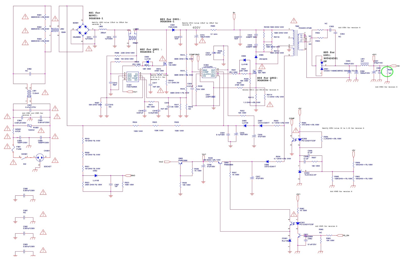
SMPS circuit Diagram


HP LP2275W – AOC LP2275W – 22INCH LCD COLOR MONITOR – POWER BOARD – CIRCUIT DIAGRAM – 715G2966A

HP LP2275w – AOC LP2275w – 22inch LCD Color Monitor – Power Board – Circuit Diagram – 715G2966A

SMPS board schematic – AOC and HP LP2275w – 22 inch LCD Monitor – 715G2966A
Horizontal Frequency - 30- 93 kHz
SMPS and BACK LIGHT INVERTER SCHEMATIC
Software Flow
1) MCU initialize.
2) Is the EEprom blank?
3) Program the EEprom by default values.
4) Get the PWM value of brightness from EEprom.
5) Is the power key pressed?
6) Clear all global flags.
7) Are the AUTO and SELECT keys pressed?
8) Enter factory mode.
9) Save the power key status into EEprom.
Turn on the LED and set it to green color.
Scalar initialize.
10) In standby mode?
11) Update the lifetime of back light.
12) Check the analog port, are they’re any signals coming?
13) Does the scalar send out an interrupt request?
14) Wake up the scalar.
15) Are there any signals coming from analog port?
16) Display "No connection Check Signal Cable" message. And go into standby mode after the message
disappear.
17) Program the scalar to be able to show the coming mode.
18) Process the OSD display.
19) Read the keyboard. Is the power key pressed?


Product features

Feature
Description
Part number
KE289A4
Type
22-in (55.9 cm) Wide-Aspect Active Matrix TFT (thin film transistor)
Viewable Image Area
22 in (55.9 cm) widescreen; diagonally measured
Screen Opening (W x H)
18.87 x 11.7 in (47.5 x 29.8 cm)
Viewing Angle (typical)
Up to 178° horizontal / 178° vertical (10:1 minimum contrast ratio)
Brightness (typical)*
300 nits (cd/m²)
Contrast Ratio (typical)*
1000:1
Response Time (typical)*
< 6 ms (gray to gray), 16 ms (On/Off)
Pixel Pitch
0.282 mm
Backlight Lamp Life (to half brightness)
30K hours
Color Gamut
HP Vivid Color support (92% color gamut)
Self Powered USB 2.0 Hub
One upstream, four downstream ports (cable included)
Native Resolution
1680 x 1050 @ 60 Hz (WSXGA+), 1.76 Million pixels
Best features
Tilt Range: -5° to + 30° vertical
Swivel Range: -45° to + 45°
Height Adjustable: Yes, range 3.9 in (10.0 cm)
Pivot Rotation: Yes

PHILIPS 286NS-05 - 28 INCH CRT TV - SMPS CIRCUIT DIAGRAM AND WORKING PRINCIPLE - PROTECTIONS

Philips 286NS-05 - 28 inch CRT TV - SMPS circuit diagram and working principle - protections

SMPS WORKING - Philips 286NS-05 Chassis Comet
When the switch TS7504 is closed, the input voltage is placed over winding 2-3 of transformer 5500, which acts as coil L2-3 (refer the circuit diagram); Via resistors R3513,R3518 and R3512 the switch is turned on for the first time. Zener diode D6502 prevents that the Ugs of the FET becomes higher than 15V. When the input voltage is on winding 2-3, there is also a voltage on winding 1-2. Via winding 1-2 the correct switching voltage is obtained.  The DC-part of this voltage is blocked by capacitor C2503. Diode D6510 acts as a protection in start-up and in short-circuit situations. During start-up the output capacitor C2515 is empty.
It takes a relative long time to charge the gate to a voltage high enough to switch on the FET. This is due to the fact the diode D6510 is conducting. When this diode is conducting, the current that would normally flow into the gate of the fet to switch on the FET, is now flowing into C2515. In this way a smooth start-up is guaranteed.
The state of the power-supply can be divided into three areas:
=> T-on; In this state the FET is conducting and energy is stored in the coil and in the output capacitor.
=> T-off; In this state the FET is non conducting and the energy stored in the coil is fed to the output capacitor.
=> T-dead; FET is out of conduction and there is no energy in the coil.
T-on; In the T-on state, switch TS7540 is switched on. When the switch is on the voltage over resistors R3514-R3515 is a direct measure for the current through winding 2-3. This is a negative voltage. When this voltage becomes below a certain level, TS7501 starts conducting and will switch off the FET. In this way it is prevented that the coil can go into saturation. This could be the case when the output voltage is very low. (Long on time of the FET). When the output-voltage becomes too high during T-on the FET will be switched off.
T-off; Due to the stored energy a current will start to flow through D6504, C2515 and winding 2-3. Due to the fact that the current is flowing through this circuit, a voltage with reverse polarity is on winding 1-2. In this way the FET remains off until the current through winding 2-3 reaches zero. Now a new cycle will start. The fet will be switched on and all starts over again.
T-dead; If the output voltage is too high (for example in a low load situation) the FET remains off till the output-voltage is not to high anymore.
Click on the schematic to zoom in
Output voltage regulation
This is done by the circuit D6501, R3509, TS7502, R3505, R3507, R3510. Transistor TS7502 can only conduct when the voltage on the base is 0V7 lower than the voltage the voltage on the emitter. This means that the voltage drop over resistors R3505 and R3507 should be 5V6(zener diode) + 0V7(base-emitter). This is reached when the output voltage exceeds the 100V. Now transistor TS7502 starts conducting, which brings transistor TS7501 in conduction. As a consequence the gate voltage of the fet becomes very low and the fet stops conducting. As long as the output voltage is too high the FET stays out of conduction.
Over-voltage protection
A disadvantage of a down converter is that if the switch becomes a short-circuit, the output voltage will increase to the input voltage. This could damage circuits. In this power-supply there is a protection to prevent this. If the output voltage becomes higher than 130V, zener diode D6514 starts to conduct. The Vin will be short circuited. This will blown the main fuse 1501 and protect in this way all the other circuits.
Short-circuit and start-up protection
The short-circuit protection works the same as the start-up protection. If the output-voltage is very low in case of a start-up or a short-circuit condition, The gate will be charged very slowly due to the fact that zener diode D6510 is conducting. So the current is not only charging the gate but is also flowing into the output capacitor. In this way it takes a few milliseconds to switch on the FET. Diode D6510 takes also care that the FET never remains in his power consuming (linear) area.
Under-voltage protection
If the output voltage is very low, it also takes a large time before the current through winding 2-3 reaches zero. The power supplied to the circuit is in this way very low and protects in this way the circuit.
Other output voltages
The output voltages +8S, +9S and +5S are made by winding 5-6. During the time that the FET TS7504 is not conducting, energy is transformed to this winding (flyback principle) and the voltages mentioned above are created. From the +9S, the +5S voltage is derived. This voltage is stabilized by  Transistors TS7505, TS7500 and zener diode D6500. D6500 is the reference voltage and TS7505 is delivering the current. When zener diode D6500 starts conducting, the voltage over resistor R3502 becomes high and a POR signal is created.