
SAMSUNG PL-42 A450P1XZD - PL-50 A450P1XZD _ Service help.
Faults to almost all Plasma TVs will be more similar. These troubleshootimg methods can be followed to other brands Plasmas too
- Check the various cable connections first.
- -- Check to see if there is a burned or damaged cable.
- -- Check to see if there is a disconnected or loose cable connection.
- -- Check to see if all the cables are connected according to the connection diagram.
- Check the Power Input to the Main Board.
- Check the voltages in and out between SMPS <-->Main Board, between SMPS <--> X, Y Main Board and between logic boards.
CHECKPOINTS BY ERROR MODE.
Symptom: The LEDs on the front panel do not work, when connecting the Power Cord.
The SMPS relay does not work when connecting the Power Cord.
The unit appears to be dead.
Major Checklist: The SMPS relay
or the LEDs on the front panel does not work when connecting the power
cord, if cables are improperly connected or the Main Board or SMPS is
not functioning. In this case, Check the following.
- Check the internal cable connection.
- Check the fuses.
- Check the output voltage of the SMPS.
- Replace the Main Board.
Symptom: The SMPS relay is repeatedly turning ON and OFF.
Major Checklist:
"In general the SMPS relay repeatedly turns On | Off by the
protection function due to a defect on a board connected to the SMPS."
- Disconnect all cables from the SMPS, operate the SMPS alone and check if SMPS works properly and if each voltage output is correct.
- If the symptom continues even when the SMPS is operated alone, replace the SMPS.
- If the symptom is not observed when operating the SMPS alone, find any defective assemblies by connecting the cables one by one.

CAUTION; When separating and
connecting the cables such as CN810, CN809, CN808, CN807 of the Main
SMPS, CN4701 of the X-Main board, and CN5707 of the Y-Main board, a
'spark' may be generated by the electric charge of the high-capacity
capacitor. Therefore, wait some time after disconnecting the Power Cord from the unit.
NO PICTURE _ AUDIO IS NORMAL
Symptom: Audio is normal, but there is no picture displayed.
Major checklist: This may happen when the Main Board is functioning, but the X, Y Main Board, or Y Buffer Boards are not.
-- The output voltage of the Main SMPS.
-- This may happen when the LVDS cable connecting the Main Board and Logic Board is disconnected.
NB: When separating and connecting the cables such as CN810, CN809,
CN808, CN807 of the Main SMPS, CN4701 of the X-Main Board, and CN5707 of
the Y-Main board, a 'spark' may be generated by the electric charge of
the high-capacity capacitor. Therefore, wait some time after
disconnecting the Power Cord from the unit.

Symptom: Video is displayed well, but there is no audio [sound].
Major checkpoints: When the speaker connectors are disconnected of damaged.
When the sound processing part of the main board is not functioning.
Speaker defect.

Symptom: A normal / cable network analog broadcast screen is blank or abnormal, but OSD is OK.
Major Checklist: Check the antenna connection settings [Air: NTSC | ATSC, Cable: NTSC]
-- Check the Power Input of the Main Board.
-- Check CVBS cable connection.

LOGIC BOARD TROUBLESHOOTING [50"]

- Y-Connector > The connector to output the Y-Drive Board control signal.
- LVDS connector > The connector to receive LVDS-encoded RGB, H, V, DATAEN and DCLK inputs from the Video Board.
- Power connector > The connector to receive Power [5V] for the Logic Board.
- X-Connector > The connector to output the X-Drive Board control signal.
- ASIC Chip > The main processor that generates and outputs the Logic Drive signal and the address data.
- DDR memory for MENCON > The memory to save the Address output data to.
- SDR memory for Frame Delay > The memory to save FCR-applied data to.
- JTAG Port > The port for uCOM communication.
- Start Screen Option pin > Select the NTSC / PAL Mode Rolling Option for the initial screen (CN2007)
- MICOM Loading 5 pin connector or UART Communication Connector > The connector to load the MICOM drive program by connecting GA-WRITER. This connector is also used to load and adjust 512k data and to connect the key-scan board.
- Flash Memory > The Flash Memory to save the MICOM data to.
- Buffer Connection connector > The connector to output the address data and the control signal to the E-buffer board at the bottom.
- Operation LED > The LED indicating that the sync and clock signals have been received normally by Logic Board. [Normal status: It blinks at 0.5 second interval].
- Buffer Connection Connector > The connector to output the address data and the control signal to the F-Buffer Board at the bottom.
- V-TOGG > The V-Sync Output Pin.
DRIVE BOARD TROUBLESHOOTING CHART
Condition
|
Description
|
Related board
|
No voltage output
|
Operating voltage doesn’t exist.
|
Power supply unit
|
No display
|
Operating voltage exist, but an image doesn’t exist on
screen.
|
Y-MAIN, X-MAIN, Logic Main, Cable.
|
Abnormal display
|
Abnormal image [not open or short] is the no screen.
|
Y-MAIN, X-MAIN, Logic Main.
|
Sustain open
|
Some horizontal lines don’t exist on screen
|
Scan IC, FPC of X/Y.
|
Sustain short
|
Some horizontal lines appear to be linked on screen.
|
SCAN IC, FPC of X / Y.
|
Address open
|
Some vertical lines don’t exist on screen
|
Logic main, Logic buffer, TCP.
|
Address short
|
Some vertical lines appear to be linked on screen
|
Logic Main, logic buffer, TCP
|
- Y-Connector > The connector to output the Y-Drive Board control signal.
- LVDS connector > The connector to receive LVDS-encoded RGB, H, V, DATAEN, and DCLK inputs from Video Board.
- Power connector > The connector to receive power [5V] for the Logic Board.
- X-Connector > The connector to output the X-Drive Board Control signals.
- ASIC Chip > The main processor that generates and outputs the logic Drive signal and the address data.
- DDR Memory for MENCON > The Memory to save the Address output data to.
- SDR Memory for Frame Delay > The Memory to save FCR-applied data to.
- GTAG port > The port for uCOM communication.
- Start screen Option pin > Select NTSC / PAL Mode Rolling Option for the initial screen (CN2007).
- MICOM Loading 5 pin connector or UART Communication Connector. > The connector to load the MICOM drive program by connecting GA-WRITER. This connector is also used to load and adjust 512k data and to connect the key-scan board.
- Flash Memory > The Flash Memory to save the MICOM data.
- Buffer connection connector > The connector to output the address, data and control signal to the E-Buffer Board at the bottom.
- Operation LED > The LED indicating that the sync and clock signals have been received normally by the Logic Board. [Normal status: It blinks at 0.5 second interval].
- Buffer connection Connector > The connector to output the address data and the control signal to the F-buffer Board at the bottom.
- V-TOGG > The V-SYNC Output Pin.
42" LOGIC BOARD

DEFINITION OF A LOGIC CIRCUIT
A Logic Circuit consists of a Logic Main Board, which decodes the
video signal encoded on the Video Board, outputs the address data
signal, and generates and outputs X, Y drive signals, and an Address
Buffer Board and outputs the address data output signal to the TCP IC.
- Logic Main: A built-in LVDS for video signal processing [W/L, Error Diffusion, APC, FCR, etc] adopted and 1 ASIC chip.
- Outputs the Address Drive IC control signal and data signal to the Buffer Board.
- Outputs the X and Y Drive Board control signals.
- Monitors the major drive voltages (MICOM circuit part); detects any surge voltage to protect the drive circuit.
- Temperature Adaptive Operating Mode [Low temperature | Room temperature | High temperature]; optimizes discharges depending on temperature.
Buffer Board >> Lower Part E-Buffer >> Delivers the data and control signal to the bottom left TCP. [Single Scan].
Lower part F-Buffer >> Delivers the data and the control signals to the bottom right TCP.
- When the PDP and Logic Board are normal, the Operating LED blinks at a half second interval. In the case, the V-SYNC and data signals are output normally.
CHECKS
- Visual Inspection >>> Check if the operating LED on the Logic Main blinks at a half second interval. If the frequency of blinking is too fast or slow, it means that the MICOM has failed to process the data properly. Therefore, have to re-load the data on to the MICOM. Load the data using GA-WRITER when the power is connected to the module.
- If no problem is found during the visual inspection , check if the drive waveform and address data outputs are normal, using an oscilloscope. {Checkpoint: The DAMPING R-NET part output of each data output terminal}
- If no Drive waveform or address output is measured, means that there is a drive problem due to MICOM data corruption, which was the reason in the Visual Inspection. In this case, re-load the data as did in the visual inspection.
- When data output is measured, but it is abnormal, and the drive waveform is abnormal, it is probably due to a short-circuit of the hardware. If the address data is abnormal, the screen may be abnormal due to abnormal data output by an abnormal operation of the DDR memory, due to an abnormal Vref voltage, or screen may be abnormal due to a short-circuit in the ass'y inside the board. The have to conduct a short-circuit test for each case.
- If the Vref voltage [the voltage of the Voltage divider] is lower than 1.25V, check resistance of the resistance output part and check if the circuit is normal. If the Vref voltage is normal, the screen operates normally.
- If the screen is abnormal, even though the Vref voltage is normal , check if there is a short-circuit by conducting a short-circuit test. If short-circuit is found is an internal one, replace the board.
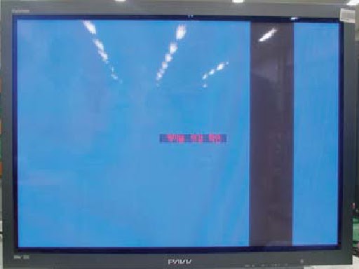
Symptom: A blank vertical cell or block appears on the screen as follows:
- Address Buffer defect: Replace the corresponding Upper | Lower Buffers. [E or F].
- COF defect: Replace the Module. (COF = Chip On Film)
===============================================================
- Symptom: A green screen appears when the TV is turned On. No image at all
- The Scale is not resetting. Replace the Main Board.
===============================================================
Symptom: The OSD box appears, but there is no TEXT.

- Incorrect program version.
- Check the version of each program.
- Replace the Main Board.
===================================================================
Symptom: A blank Upper | Lower block appears on the screen.
- Upper or Lower Y-Buffer defect.
- Replace corresponding Upper | Lower Buffers. [E or F]
===================================================================
Symptom: Either the Main or Sub-Picture does not appear.

- Replace the Main Board.
==================================================================
Symptom: A vertical Green line appears on the screen.

- The SMPS out voltage is incorrect.
- Adjust the SMPS voltage, according to the voltage printed on the module label.
=================================================================
Symptom; Dim screen. Blurred in red.

- X-Main board defect.
- Replace X=main board.
=================================================================
Symptom: A blank screen appears.
- Replace the Y-Main Board.
==================================================================