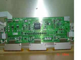
AOC PDP 4294LV1 _ PWBs _ FUNCTIONS GUIDE
X/BD
- Receiving LOGIC signal from CONTROL B/D and make ADDRESS PULSE(generates Address discharge)by ON/OFF operation, and supplies this waveform to COF(data).
COF SEPARATING
- Lift up lock as shown in arrow.
- Pull COF as shown in arrow
Z SUSTAIN B/D
- Make SUSTAIN PULSE and ERASE PULSE that generates SUSTAIN discharge in panel by receiving LOGIC signal from CONTROL B/D.
- This waveform is supplied to panel through FPC(Z). *composed with IPM,FET,DIODE, electrolytic capacitor ,E/R coil.
FPC SEPARATING
IPM stands for (Intelligent Power Module)
E/R stands for(Energy recovery)
Z-SUSTAIN BOARD

Y DRIVE B/D
- This is a path to supply SUSTAIN ,RESET waveform which made from Y SUSTAIN B/D to panel through SCAN DRIVER IC.
- Supply a wave form that select Horizontal electrode (Y SUSTAIN electrode) sequentially. potential difference is 0V between GND and Vpp of DRIVER IC in SUSTAIN period. being generated potential difference between GND and Vpp only in SCAN period.
- In case of 42” V6 use DRIVER IC IC 8 EA (TOP, BOTTOM: each 4EA)
Y-SUSTAIN B/D
- Generates SUSTAIN,RESET waveform, Vsc(SCAN)voltage, and supplies it Y DRIVER B/D.
- Composed with IPM,DIODE, electrolytic capacitor ,FET. [Field Effect Transistor]
CONTROL BOARD
- Creates signal processing (Contour noise,reduction ISM,..) and an order of many FET on/off of each DRIVER B/D with R,G,B each 8bit input.
- Use 3.3V/5V 2 kinds of power.
DC/DC CONVERTER PART
- Being impressed 5V, Va ,Vs, DC/DC converter makes 5V,Va,Vs,Vset_up,Vsc which is essential for each B/D.
- There is no DC/DC B/D in model 40/42 1 POWER B/D). 50 & 60 embedded DC/DC B/D separately because of high power consumption.
FPC [Flexible Printed Circuit]
- Supply a driving waveform to PANEL by connecting a PAD electrode of PANEL with PCB(Y and Z).
- There is two type of this for Y B/D. One is single-sided, another is double-side. These are having pattern on it * for Z B/D, there is no pattern , single-sided, and Beta type(all of copper surface).
FFC [Flat Flexible Cable]
- For connecting a Logic signal between B/D and B/D. There is 0.5mm pitch,50pin type 1mm pitch ,30pin type.
COF [Chip On Film]
- Supply a waveform which made from X B/D to panel and select a output pin that is controlled by COF when be on or off. 96 output pin per IC.
- The more the resolution higher, the less spare space where can set IC on it in B/D. without using IC PACKAGE, we can use a BARE IC , so we can get IC with LOW COST
- Because we do not solder IC on PCB directly, a soldering defect rate decrease.


