 TOSHIBA - DLP PROJECTION TV_ 46HM84_52HM84_52HMX84_ System Control Circuit_Troubleshooting

TOSHIBA - DLP PROJECTION TV_ 46HM84_52HM84_52HMX84_62HMX84_ Video and Audio Signal Flow
The
2004 DLP televisions are separated into two categories, one being the HM84 HD
monitor series and the HM94 HD Integrated series. This will cover the basic
design and troubleshooting of the audio and video section of the HM84 HD
monitor series. This module is divided into three major areas. We will first
discuss the specifications of the input signals and display. Then we will move
into the overview and block diagrams of the Audio & Video signal flow. The
last portion of this the module will cover troubleshooting the audio and video
NTSC Tuner
Receives the NTSC signal format (525
lines interlaced scanning) for consumer televisions in the United States. A
typical NTSC tuner receives VHF channels 2 to 13, UHF channels 14 to 83, and
Cable TV channels mid band A8 to A1 and A to I, super band J to W, hyper band
AA to ZZ - AAA and BBB, and ultra band 65 to 94 and 100 to 125.
Composite Video
Refers
to a video signal where both the luminance component and the color component(s)
are transmitted on a single wire or broadcast in a limited bandwidth. The
luminance and color information must be separated before the picture can be
displayed.
S-Video (also called Y/C)
A video signal transmitted as two
sub signals requiring two separate wires: luminance (technically referred to as
Y) and color (C). Luminance is composed of black and white video signal and the
sync signal. Chrominance is the color (modulated on a carrier) video signals.
Component Video
Video and Audio Signal flow

Note that the Rear A/V jack
panel is a hub for most signal inputs, processing and switching. Knowing this,
can trace signals to and from the Rear A/V jack panel to its input or output
circuits. Additionally, when a problem with an input, output, or the Rear A/V
jack panel itself is discovered, the power distribution can be investigated for
possible supply problems. Then if no supply problems are discovered, the board
at a fault can be repaired.
This unit is, in some circuit areas, only serviceable
to modular level. However it is sometimes an advantage to service non-difficult
obvious trouble to component level and repair the problem rather than replace
the entire circuit board. This becomes an important aspect if the unit is out
of warranty. An interconnect diagram of the signal paths in this unit. Listed
on this block are plug numbers, as they are listed on the board, and in the
schematics, for both ends of the path.

Rear AV Board connections and components.

All input sources are routed
through the Rear A/V board. This is important to mention because in past PJTV
models, the A/V switching IC, QV01, was located on the signal board. As shown
in Figure 3, QV01 is located just above the jack panels. Sub-picture processing
is done here as well by IC QY501 and QY100. QS01 located toward the lower right
hand side, switches the audio selection for the inputs. One interesting area
includes service ports used to access data and service protocols.
Voltage requirements consist of a 9V source and two
5V sources. These voltages are supplied via connector BB70 through the
IMA/tuner board. This should be noted since the Rear A/V is not directly
connected with the power supply board. Looking at the left side of Figure 4,
the input sources are shown with the corresponding connection, if applicable to
that particular input source. Composite
and S-video sources are labeled E1, E2 and E3. Figure 4 illustrates the signal
path through QV01. Sub picture composite video output at pin 51 is routed to
QY100 for comb filtering. Sub picture (PIP or POP) Y/C and Y, Cb, Cr is routed
directly to QY501 for signal processing of the sub picture. The output
from QY501 is a Y, Cb, Cr signal. Both the main and
sub picture signals are routed through connector PV04 to the
DBEP/Signal/G-Hyper Board.
At the lower right, note the service port connections
and plugs are not related to nor directly connected to any video or audio
signal paths. This allows direct connection to the data chips located on the
DBEP/Signal/G-Hyper Board.

TOSHIBA - DLP PROJECTION TV_ 46HM84_52HM84_52HMX84_Signal Processing
TUNER IF / IMA / AC IN BOARD
The board contains three circuit areas of
the TV. These include AC input, Tuners and Audio. Starting with the left side
of Figure 5, the AC input is located here along with F801. The area outlined in
white is the “HOT” GND area and the components located within are not directly
related to the other circuits contain on this board. The audio amplifier IC601
is mounted on the heat sink just to the right of the AC line input area. Just
below IC601 is preamplifier IC663, BB71 is the connection to the Rear A/V
board. The remaining three components on this board are the main (H001) and sub (HY01)
tuners and the IF/Main Audio (IMA) processor H002.
Removing five screws mounted along the outside
perimeter of the board is required for board removal. However, the Rear A/V
board will need to be removed first.
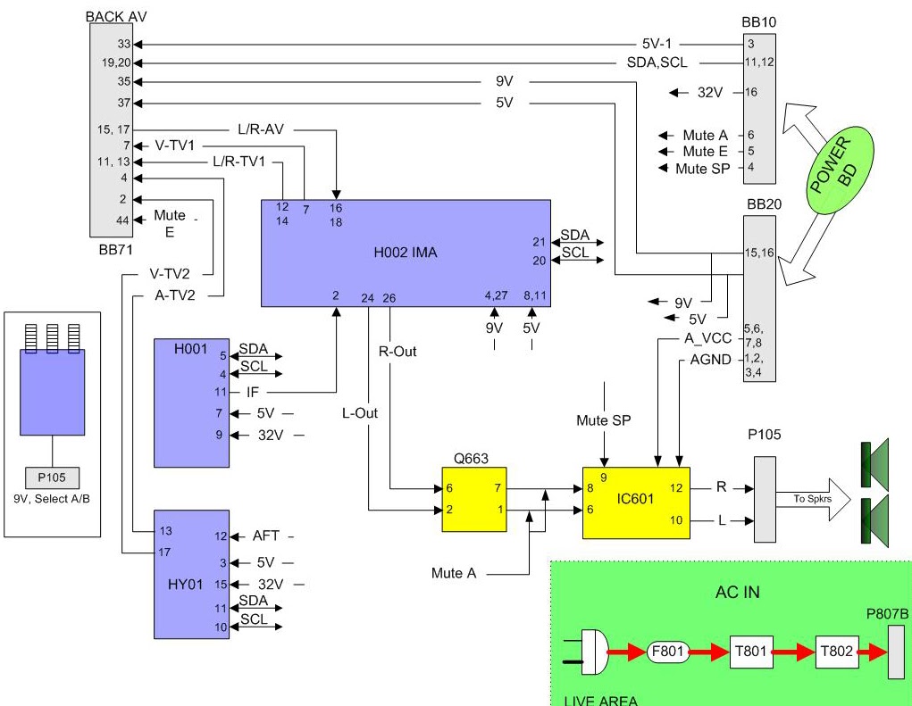
Connection BB71 to the Rear A/V board is shown. Audio
from HY01 and H002 circuits are routed through BB71 to the Rear A/V
board for switching purposes. The selected audio is
then looped back to the IMA circuit H002. The IMA (IF Main Audio) processes the
TV’s audio volume, bass, treble, etc. The IMA audio output is then sent to
preamplifier Q663 then applied to IC601 for amplification to the speakers. Mute
circuits are implemented in the preamp and amplifier circuits, details will be
covered in the troubleshooting area of the manual. The sub-audio, labeled
A-TV2, is a mono signal. The audio signal is not routed back to H002, but
applied to the monitor audio output jacks. Using sub, PIP/POP, audio feature of
this model, the user has the option of selecting the monitor jack audio to be
either main or sub audio.
Two video sources are developed on this board. Main
tuner H001 outputs an IF signal to H002. The signal is demodulated and decoded
into video and audio signals. The composite video signal is then routed from
H002 pin 7 as V-TV1 to the Rear A/V for switching purposes. The sub-picture
developed in HY01 is sent as a composite signal to the Rear A/V board for
switching as well. The gray area at the bottom of Figure 6 shows the AC IN path
block diagram, again not directly related to the audio or video.
SIGNAL / G - HYPER / DIGITAL BACK END PROCESSOR

AKA (Also Known As), the DBEP, this board
incorporates several circuits discussed in past PJTV models as “separate”
circuits. In this training module, “Signal” and “G-Hyper” along with this
board. The TV micro and DLP control
micro are located here, along with keypad and IR receiver connections.
The actual board is shown, however the PC board takes
on a much different look due to metal shielding surrounding it. Disassembly of
the shields is done by removing six (6) screws holding the to halves together.
No soldering is required to remove or replace the shielding. A small pair of
needle nose is required to straighten eight (8) tabs in order to fully release
the shields. In most cases, troubleshooting can be done directly from the
connections at top and bottom without removing any shielding. The
DBEP/G-Hyper/Signal board is a replacement module, so troubleshooting to
component level in not necessary.
Arrows and IC’s outlined represent the video signal
flow. This gives a brief overview of the actual board and component locations
dealing with the signal flow.

TOSHIBA - DLP PROJECTION TV_ 46HM84_52HM84_52HMX84_ SIGNAL PROCESSING
The main signal, either composite or component is
sent to IC210. The TC90A92AFG IC
features a built-in 3-line digital comb filter and 3D luma and chroma noise
reduction system. The chip embedded with 4-Mbit of internal frame memory
includes an integrated digital multi-standard color decoder with picture
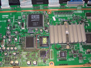
improvement functions. The output is a digital Y, Cb, Cr output. The Genesis chip, IC203, processes and
formats the signals to a 1920X1080i format. The GM6015 Genesis chip is a video
converter that incorporates deinterlacing with scaling and aspect ratio
conversions for standard and high definition signals. The output is in 4:2:2
format, basically stating four of the luminance pixels are sampled, two of the
R-Y pixels are sampled and two B-Y pixels are sampled.
IC301 is the Digital Back-End Processor. The TC90A94TBG is an RGB processor with
built in scaling, signal conversion, and high image quality functions. The OSD
is incorporated here from the main TV micro as an RGB signal. The output is a
digital RGB 30 bit single-phase signal. Power supply source includes 3.3V, 2.5
V and 1.5V. Low Voltage Differential Signal, or LVDS, is used to transfer the
signal to the Talen Light Engine at IC311.
TROUBLESHOOTING
When troubleshooting any video or audio related
issues, keep in mind the logical flow of the signal paths. A couple of areas
should always be considered; one example would be user settings. It is
important to check user settings prior to any troubleshooting. For example, the
speakers could be set to the “off” or external position causing a perceived no
audio condition or video inputs could be locked or blocked resulting in a no
video condition. Another area is simple A/V connections to the unit. These
problems can range from defective A/V cables to simply having the incorrect
connection. Ever had a hum from a unit to find the video signal is connected to
one of the audio input channels?
VIDEO
When troubleshooting any video or audio related
issues, keep in mind the logical flow of the signal paths. A couple of areas
should always be considered; one example would be user settings. It is
important to check user settings prior to any troubleshooting. For example, the
speakers could be set to the “off” or external position causing a perceived no
audio condition or video inputs could be locked or blocked resulting in a no
video condition. Another area is simple A/V connections to the unit. These problems
can range from defective A/V cables to simply having the incorrect connection.
Ever had a hum from a unit to find the video signal is connected to one of the
audio input channels?
Once have
determined a signal loss, always check other available inputs. This technique of troubleshooting will help
identify the board or circuit causing the problem.
Once have narrowed the search down to one, or
multiple, inputs, it is recommended to input a source video or audio signal you
are familiar with.
This is where logic and simple troubleshooting
procedures should be taken into account, assuming there are not any error codes
from the front LED indicators. If the
lamp were not working, this would definitely cause a no picture condition.
The next item would be if the TV has an OSD
(On-Screen Display). This would have been apparent when verifying the user
settings. If the OSD is present, at least the DPEB/GHyper/ Signal Board is
sending an output to the light engine.
Check the DBEP/G-Hyper/Signal inputs. Figure below
shows the schematic cut away of the connector PJ16. The circled numbers
represent the signal troubleshooting area and figure 10 shows the waveform
viewed with an oscilloscope. A signal here will indicate the problem is before
to the DBEP/G-Hyper/Signal Board. Using the supplied diagrams and circuit
schematics, one could logically pin point the trouble area.

LIGHT ENGINE
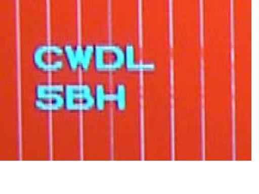
Service Tip - White Lines in Picture: For uniform
vertical white lines (about 1 inch a part) extending from the top and bottom of
the screen, as shown in Figure. A red
raster is shown in the figure for photographic reasons. However, the lines are
very noticeable while viewing a normal picture. Notice the on screen display (OSD)
is good, but the lines still appear within the OSD. To the right of the letters
CWDL, the lines break up where a letter would be.
TIP: With the
quick restart feature “on”, the unit will be in a restart standby mode for 5 to
6 minutes. During this restart standby time, the lamp wattage is reduced to 30%
and the front green LED lamp will flash. This indication of the LED is to
confirm the unit is in the restart standby mode. In a dark room, the picture
will appear to have an after glow effect. This can be used to your advantage
for troubleshooting. If a picture defect is present and you suspect the problem
to be the light engine, you should see the same defect during the restart standby
time. Basically, the only circuit in operation will be the light engine. Again, the TV must be in a very dark
environment to achieve this type of evaluation.

AUDIO
In the case of no audio and having checked the user
settings, go directly to audio amplifier (IC601) and check for inputs and
outputs along with voltage supplies. High
wattage areas are always a good starting point. Shown in Figure are the pin connections for IC601. IN-1 is
the left audio channel and IN-2 is the right audio channel. The outputs from
Q601 are pin 2 (left audio) and pin 12 (right audio). When probing the output, ake
sure the ground side is connected to either pin 4 or 10, depending on the
output being tested. The audio output does not reference a common ground.
Another technique for testing the audio signal is to
scope the variable audio output located on the rear of the unit. A signal here
will indicate the audio signal is present from the pre-amp driver (IC663).

MUTE
The next following diagrams will cover mute controls.
All mute signals are generated from the main micro and this TV has several
selections of mute control. One mute control is through the TV’s menu as main
speaker “on” or “off”. Another control is the mute key located on the remote
control. This feature has three selections: ½ mute, mute and off. The ½ mute is
an I2C controlled feature to the IMA board H002, not part of the any mute
circuits. Basically stating, when the ½ mute is selected, the IMA circuit
receives this command from the main micro and the IMA circuit reduces the audio
level by ½ depending on the initial audio level.
Another audio mute is done during channel change and
no signal conditions; this is called the Mute–A line. See Figure 15. A signal
from the main micro on the Mute-A line will apply a voltage to the base of
transistors Q681 and Q682. With these NPN transistors “on”, the audio output
lines from the preamp IC663 is pulled to a ground potential and no audio signal
is input to IC601 amplifier. Under
normal conditions, the base of transistors Q681 and Q682 will be 0 volts.

Speaker Mute is a feature located in the user menu,
allowing the speakers to be turned “on” or “off”. The control line is referred
to as SP_MUTE in the schematics. See Figure 16 for circuit details. Checking
this circuit can be as easy as checking the voltage at pin 9 of IC601, as shown
in Figure 16 with the “5V=Mute On”.
Step back for a moment and follow the SP_MUTE signal
sent from the micro. The SP_MUTE voltage is applied to the base of Q614,
allowing it to conduct. This removes the 5V line from the base of Q613 and
turns “off” this PNP transistor. This allows the 5V potential to be applied the
pin 9 of the audio amplifier. Pin 9 is IC601’s internal mute circuit. In a
normal condition, Q614 is “off” and Q613 is “on”.

CONTROLS:
At first glance, the 2004 DLP Television system control area looks rather complicated. However, by viewing system control as two separate, but related, areas, we can easily clear the confusion generated by the use of 2 microprocessors and 2 EEPROMs.
Both are located on the G-Hyper/Signal/DBEP circuit board.
But, before panic sets in, let us first mention that a problem with either
section can be resolved by replacement of the circuit
board. The difficulty lies in properly assessing the situation in order to make
the determination that the board requires replacement.
Being on the subject of replacement parts makes this
a good time to insert Table 1, a list of G-Hyper/Signal/DBEP circuit board part
numbers – by model.
MODEL PART NUMBER
46HM84 23148133
52HM84 23148131
52HMX84 23148134
62HM84 23148132
62HMX84 23148135
The main System microprocessor (IC601) is still the
central component of system control. In some fashion, it communicates with all
other circuit areas to control functionality and monitor circuit operations.
The second microprocessor, IC501, is basically a message
handler, relaying information from the TALEN light engine to the main system
microprocessor. Oddly enough, while IC501 is called the Backend Process (BEP)
micro, it is not in direct communication with the Digital Backend Processor [DBEP]
chip, IC301.
The main system micro is central to control
operations

The M306V7MG-082FP chip used is a 100-pin single-chip
flat pack microcomputer designed for use in Closed-Caption televisions, such as
the 2004 DLP product line. The chip, with 256K of internal ROM
(read-only-memory), 10K of RAM (random-access-memory), 60K OSD ROM, and 2.2K
OSD RAM, is a mask ROM version. Meaning that the IC’s basic programming is done
during the fabrication process, is not expected to change, and is not user
programmable. The chip operates within
the parameters defined by the initial programming. That is not to say, however, that televisions using this type of
chip are locked into one-way performances. The user can change certain aspects
of operation, with
the
data related to those changes being stored in the system EEPROM, IC603 (Figure
3). Rarely does a customer watch a television in the original out-of-the box state.
Each time a change is made, be it as simple as a volume level adjustment, that
data is stored in IC603.

The AT24C256N EEPROM shown in Figure 3 is a 256K bit,
8 pin PDIP (Plastic Dual In-line Package) with an operating voltage of 2.7V
(max. of 5.5V). Two-way communication between this chip and the system
microprocessor allows user controlled data to be written to the EEPROM, stored,
and fed back to the microprocessor at start-up. The process ensures that when a
customer turns on his/her television, it looks and sounds like it did when it
was turned off. Communication takes
place over the Serial Clock (SCL) and Serial Data (SDA) lines that compose the
I2C bus running throughout the 2004 DLP television. While Figure 4 shows us that the information
traveling on this bus is dispatched and
received on the G-per/Signal/DBEP circuit board, it is all routed through the
Power Supply circuit board before being detoured to the various final destinations.
Illustrates the locations of the key ingredients in
microprocessor operation.

SUPPLY VOLTAGE
Two operating voltages are supplied to IC601 from the
Standby power supply. Both are required for proper operation, but each powers a
separate area of the IC.
- The system I/O area of IC601 is powered by 5V (5V-1 line) at pin 99 (VCCE). The 5V supply is generated by the Standby power supply
2. The
chip’s internal logic area is powered by 3.3V applied to pin 16 (VCCI).
The voltage is supplied by regulator IC606 (pin 1) and is derived from the 5V standby voltage.
GROUND
To
form a completed circuit, IC601 is grounded at pin 14 (VSS).
TIMING
Clock generation is accomplished by connecting 10Mhz
crystal oscillator X6001 between pins 13 (XOUT) and 15 (XIN).
Regulator IC606 (pin 4), supplies the reset signal
needed to refresh the microprocessor each time the unit is turned ON.

COMMUNICATION
Each time the unit is powered ON, information is
exchanged between EEPROM IC603 (pins 5 & 6) and system microprocessor IC601
(pins 28 & 31). Clock (TV_SCL0) and data (TV_SDA0), shown in Figure 8,
information is exchanged to sync the two chips and load “last status”
information into the microprocessor. This
“last status” information contains all user settings memorized the last time the
unit was powered OFF.

BRANCHING OUT
The system microprocessor begins transmitting to and
receiving information from all other circuits connected to the I2C bus. Activity on the clock
(SCL1) and data (SDA1) lines, IC601 pins 29 & 30
respectively, can be monitored with an oscilloscope. Expect a very busy 5Vp-p
waveform on either line. A 3V DC level will be measured with a standard
voltmeter, with minor fluctuations in the DC level indicating activity.

As the G-Hyper/DBEP/Signal circuit board is
completely shielded and replaced as a module, suspected problems can be
evaluated most easily by checking the central connection point. In the 2004 DLP
television, the power supply circuit board serves as that central point, or
hub. Referencing the block diagram of Figure 10, we see that connector PJ13
(pins 6 & 7) carries I2C information to the power supply circuit board PA01
(pins 6 & 7).
A look at the actual interconnection between the two
circuit boards, shows us that troubleshooting can be accomplished with less
difficulty by checking
the PA01 side.
The I2C bus reaches beyond the power
supply circuit board to connect with the Tuner IF/IMA circuit board through the
BB11 to BB10 board-to-board
connections. Clock (pin 12) and data (pin 11) information, used by the Tuner
IF/IMA circuits to control tuning and audio processing, is also forwarded to
the Rear A/V section over the BB71 to BB70 connections (pins 19 and 20) to
accommodate the video and audio switching functions.

Taking things a step further, Figure 13 shows us the
connections to main tuner H001 (pins 4 & 5), IMA block H002 (20 & 21),
and sub-picture tuner HY01 (pins 10 & 11).

[Click on image.
Right click on the enlarged image, save image as, to a folder (My
document > My Pictures).
From the connections to H002, the I2C lines continue through the BB71 to BB70 connector (pins 19 & 20)
to the Rear A/V circuit board. Once on the Rear A/V circuit board, Figure 14
shows us that the lines are routed to:
# Video switching IC QV01 [pins 45&46]
# Audio switching IC QS01 [pins 22 & 23]
SUB-PICTURE PROCESSING

As shown in Figure above, the I2C bus is also directed from the power supply circuit board through PV13
(pins 1 & 2) to HDMI module P202 (pins 1 & 2). I2C control of the HDMI module establishes not only functionality of the
module, but also the necessary permissions required for viewing copy protected
content using this all digital input.
As shown in Figure, the I2C
bus is also directed from the power supply circuit board through PV13 (pins 1
& 2) to HDMI module P202 (pins 1 & 2). I2C
control of the HDMI module establishes not only functionality of the module,
but also the necessary permissions required for viewing copy protected content
using this all digital input.

There are two minor exceptions to the central hub
troubleshooting theory. Operations
carried out by remote control (IR) or manual keypad are transmitted to the
microprocessor via direct connections to the G-Hyper/DBEP/Signal circuit boards.
The block diagram of Figure 16 shows us that keypad operations are carried over
PB91 (pins 5 & 6-keypad side) and PJ18 (pins 5 & 6–Signal side).

Both signals, Key 1 and Key 2, enter IC604 (pins 6
& 7) where they are mixed and output (pin 5) as C_KEY_AB_SW (Figure 17)
before entering the microprocessor at pin 78.

KEYPAD
The keypad used in the 2004 DLP television
relies on touch controls, rather than mechanical switches. Additionally,
control via keypad is accomplished digitally through IC’s QA91 and QA92.


Key 1 Signals – QA91 Key 2
Signals – QA92
POWER (pin 22) CHANNEL DOWN (pin
22)
MENU (pin 21) CHANNEL UP (pin
21)
VOLUME DOWN (pin 19) EXIT (pin 19)
VOLUME UP (pin 18) TV / VIDEO (pin 18)
IR RECEIVER
The IR receiver, KB01, is powered by the 5V-1
(Standby) supply line to pin 4 of PB22. When KB01 receives a command from the
hand unit, the signal, carried between PB22 and PJ17
(G-Hyper/DBEP/Signal circuit board), travels to the system microprocessor (pin
7) via the RMT IN line at pin 3. The
system microprocessor also outputs the RMT OUT signal (pin 26) to IR transmitter
DB03 (pin 1 of PB22) for IR Blaster functions.

In addition to issuing control commands from inputs
received, the system microprocessor also monitors other circuit areas of the
2004 DLP television. Either directly or
indirectly, the system microprocessor keeps a watchful eye on certain areas
(Figure 20), shutting the unit down if problems are sensed. Technical Training module DLP-04-4 Power
Supply and Shutdown took great pains to identify and explain the individual
protection circuits, so there is no need to repeat that information here. For
the sake of review, however, we will provide a list of those circuits in this
text.
- Lamp door switch.
- Color wheel exhaust fan rotation.
- Color wheel temperature sensor.
- DMD fan rotation.
- DMD temperature sensor.
Of the five circuits listed, three are directly
monitored by the system microprocessor.
LAMP DOOR SWITCH
The circuit operates by monitoring the door switch in the lamp assembly. If the lamp door is left open, a signal is sent to the system microprocessor (pin 49) on the POWERCTL line, invoking a shutdown. A signal is also sent to pin 19 of the system microprocessor (DOOR_OPEN) to identify this particular shutdown.

Color wheel & DMD fan rotation


The circuit operates by monitoring the door switch in the lamp assembly. If the lamp door is left open, a signal is sent to the system microprocessor (pin 49) on the POWERCTL line, invoking a shutdown. A signal is also sent to pin 19 of the system microprocessor (DOOR_OPEN) to identify this particular shutdown.

One circuit linked to the system microprocessor at
pin 49 monitors both the DMD fan and the Color wheel exhaust fans. In the event
fan rotation ceases, a signal is sent down the POWERCTL line to trigger unit
shutdown. As this is the same line used to trigger a lamp door open shutdown,
the microprocessor relies on the above mentioned DOOR_OPEN signal to pin 19 to
be the determining factor in identifying the type of shutdown.

The remaining shutdown circuits are indirectly
monitored by the system microprocessor by way of communication with the Backend
Process (BEP) microprocessor, shown in Figure 23. Another single chip microcomputer,
the 100-pin M30626FHPGP is up to the task of relaying real-time temperature
information to the system microprocessor for the purpose of protecting against
over-temperature situations.
Color Wheel and DMD Temperature
BEP microprocessor IC501 monitors color wheel and DMD
temperature at pins 1 (FANDAC2) and 2 (FANDAC1), sending that information to
the system microprocessor. IC601, in turn, uses the information to alter fan
speed to accommodate changes in temperature. Should the temperature rise to harmful
levels, the system microprocessor shuts the unit down to avoid damage.

BEP Microprocessor
The BEP
microprocessor also communicates with the DMD panel and the lamp ballast supply
to accomplish other tasks, as instructed through communication with the system
microprocessor. These tasks involve altering the operating parameters of the
lamp ballast supply and the DMD panel to coincide with user preferences
regarding lamp power usage and video display choices. EEPROM IC503, the same
type used by the system microprocessor, assists the BEP microprocessor in these
tasks by providing the same functions IC603 provides to IC601.
Two Way Communication
The BEP
microprocessor also communicates with the DMD panel and the lamp ballast supply
to accomplish other tasks, as instructed through communication with the system
microprocessor. These tasks involve altering the operating parameters of the
lamp ballast supply and the DMD panel to coincide with user preferences
regarding lamp power usage and video display choices. EEPROM IC503, the same
type used by the system microprocessor, assists the BEP microprocessor in these
tasks by providing the same functions IC603 provides to IC601.
SERVICE MODE CHECKS
This type of communication allows for adjustments,
updates, troubleshooting, and occasional repairs. While access to the system
microprocessor offers convenience in these areas, it must be noted that other parameters
of operation may inadvertently be changed if extreme caution is not used
whenever the feature is activated.

The upper level of data, stored in EEPROM IC603 and
used by the system microprocessor, can be accessed and manipulated, as
necessary, by entering unit service mode in the manner described in the unit
service manual. Alterations to data at
this level may be required during general service procedures and are typically
accomplished by remote control. While inadvertent changes in this area are not
generally life threatening to the unit, functionality and features may be negatively
influenced. The best practice when working with this level of data involves
recording address and data values prior to making adjustments to the stored
data. Changes to the stored data must be saved, as described in the unit
service manual, following any necessary alterations.
Service Mode Entry Method
- Press the "Mute" button twice on the customer remote control. Press "Mute" button again and Hold it while pressing the "Menu" button on the front panel of the TV set.
- A Service Mode indication will be given by the presence of an "S" displayed in the upper right of the screen.
- Press "Menu" button on the remote control, or "Menu" button on the front panel of the TV to enter the adjustment Menu.
- Use Ch UP / Ch Dn button to access the selected register requiring change. In the case DMD Bias the display will indicate "DMDB". Color Wheel Delay will use display "CWDL" and "CWDH".
- Use Vol Up / Vol Dn to adjust the value of the selected register.
- To "EXIT" service mode, press the Power button to turn Off the TV Note: With DLP product there is a normal delay for picture to return with a quick On and Off cycle.
The 2004 DLP television includes service interface
ports, added to the Rear A/V panel for convenience. The ports (Figure 26) are
designed for use with the Toshiba Service Interface Tool (P/N – IICB) and
accessible to service so equipped following the removal of the access panel
located above S-Video inputs 1 and 2. Use of the ports constitutes direct
communication with the system EEPROM, BEP EEPROM, and G-Hyper functional memory
over the I2C bus. The service interface tool can be used to
write initial or updated data to these areas, if so required. As much of the
stored data in these areas is model specific, take care to select the correct
data files to be written. For diagnostic purposes, data can be copied and saved
as a file to be written to another unit or, under certain circumstances, sent
to Toshiba for evaluation.
Complete instructions regarding these issues
will be included with the Toshiba Service Interface Kit –P/N IICB

Flash Memory
The actual system microprocessor programming (mask)
can be re-written (updated) if the need arises. Figure shows Flash ROM IC609,
used for just such a purpose.
SOFTWARE REVISION FOR CLOCK TIME LOSS PROBLEM
If
On-Screen Clock looses approximately 7 minutes every 24 hours, replace
IC609 [EPROM] on the OPSS / Scaler Module using part number [23085328].
This device uses a plug in socket.
